EE 2212
Fall 2021
30 September and 7 October
Experiment 3: Operational Amplifier
Circuits
Note 1: This will be a two
week experiment.
Note 2: The report will be
due Thursday, 14 October
Note 3: The two week experiment
will be evaluated on a 40 point rubric (double all values on the 20 point
rubric document.
Note 4: You are limited to
six pages, besides the title and abstract page.
Note 5: I will provide an
overview of the op amp SPICE models for both time and frequency domain
simulation.
Note 6: I have divided this
experiment into a non-frequency dependent
and frequency dependent set of circuits
Note 7: Circuit wiring
neatness will really pay off in getting quality and consistent experimental
results.
PURPOSE (Non-Frequency Dependent)
To implement the designs of:
Ø Two
versions of an inverting operational amplifier (Figures 1 and 3)
Ø A
non-inverting operational amplifier
(Figure 2)
GENERAL COMMENTS
Run the
SPICE time-domain simulation with a VSIN generator and the frequency-domain
simulation with a VAC generator.
Use the μA741 model in the
eval.slb library. Print the waveforms of
the inputs and outputs on the same set of axes. You will need the following
information from your SPICE simulations in order to complete this lab:
Ø TRANSIENT analysis
for a sinusoidal input
Your hardware realizations designs should
minimize the use of series and parallel resistors to meet the voltage gain specifications. It is more desirable to come close with
standard value components and use the exact measured numbers in your circuit
simulation.
PRELAB
Ø Specify
the component values to meet the
indicated specifications for Circuits 1 and 2 . You should come to the lab with
a list of the components you will need to meet the specifications.
Ø The
derivation, in your notebook, of
the voltage gain Vo/Vs for Circuit 3
using summing point constraints. This is also a good exercise in the use
of nodal analysis. (Look at the R2, R3, R4 node)
PROCEDURE
Refer to the mA741
data sheet on the class WEB page uA741.pdf.
Observe, you are using the 8-pin DIP (Dual-Inline Package), second package style from the top. This package is also sometimes
called the MINIDIP. Also note that the mA741 has certain requirements with respect to
allowed resistance values that includes all
resistors in your design must be greater than or equal to 2 kW. Do not
include the 10 kW
offset voltage potentiometer.
Use ± 12 volts for the power
supplies. Verify that the polarities
are correct or ![MM900336554[1]](./Experiment3OperationalAmplifierCircuits_files/image002.gif) you will create a classic embarrassing odor
you will create a classic embarrassing odor![]()
![]() not correctable with Old
SPICE (pretty good pun!) body wash.
not correctable with Old
SPICE (pretty good pun!) body wash.
Your designs should be
supported analytically and by SPICE simulation results. You should record all key oscilloscope
waveforms on your flash drive as support
for your laboratory report.
1. For
Figure 1. Design and test an inverting amplifier with a low-frequency voltage
gain of 20 dB.
Ø Start
with a 1 kHz sinusoidal input
voltage. The input voltage level is not
critical as long as you do not observe clipping on your output waveform.
Ø Experimentally
verify your design and simulation results in the time domain.
Ø Experimentally
determine the input signal level when
“clipping” of the output waveforms occurs.*
Ø Observe
the resultant transfer
characteristic. The transfer
characteristic is a plot of Vout versus
Vin. In order to see the transfer
characteristic on the oscilloscope, you will need to change the display to “XY”
mode. You may use the scale controls to
adjust the axes accordingly. Also verify
your voltage gain and phase shift measurements using the transfer
characteristic. Note the negative slope
is indicative of the low frequency 180°of phase shift in an inverting
amplifier.
Ø Measure
and plot the voltage gain in dB as a
function of frequency, and q(jf), which is the phase shift as a function of
frequency, through the amplifier circuit, and compare your results with the
SPICE AC simulation. Extend your
measurements to a 10 kHz or so. Plot
the results as you take your measurements.
Note that if the Greek (Theta) q(jf) printed out as q(jf), your WEB browser
and/or word processing program does not translate symbol font correctly.
*Go
slow in increasing the amplitude of Vs! Do not overdo the input voltage to
observe clipping because if your input becomes too large, you will damage the mA741
and create embarrassing odors.
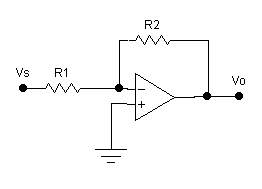
Figure 1 Inverting
Operational Amplifier Circuit
2. For
Figure 2. Design and test a non- inverting amplifier with a low-frequency
voltage gain of 14 dB.
You are essentially repeating the procedure for
Figure 1.
Ø Start
with a 1 kHz sinusoidal input
voltage. The input voltage level is not
critical as long as you do not observe clipping on your output waveform.
Ø Experimentally
verify your design and simulation results in the time domain.
Ø Experimentally
determine the input signal level when
“clipping” of the output waveforms occur.*
Ø Observe
the transfer characteristic. The transfer characteristic is a plot of Vout versus Vin. In order to see the transfer characteristic
on the oscilloscope, you will need to change the display to “XY” mode You may use the scale controls to adjust the
axes accordingly. Also verify your
voltage gain and phase shift measurements using the transfer
characteristic. Note the positive slope indicative of the low frequency 0° of
phase shift.
Ø Measure
and plot the voltage gain in dB as a
function of frequency, and q(jf), which is the phase shift as a function of
frequency, through the amplifier circuit, and compare your results with the
SPICE AC simulation. Extend your
measurements to a 10 kHz or so. Plot
the results as you take your measurements.
*Go
slow in increasing the amplitude of Vs! Do not overdo the input voltage to
observe clipping because if your input becomes too large, you will damage the mA741and
create embarrassing odors.
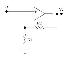
Figure 2 Non-Inverting
Operational Amplifier Circuit
3. Another
Inverting Amplifier Configuration. Refer
to Figure 3.

Figure 3 Another
Inverting Operational Amplifier Circuit
Use all 10 kW
resistors. Verify experimentally and
using SPICE, the voltage gain at 1 kHz .
Use both a time domain and transfer characteristic representation of
your work. Frequency response
measurements are not required.
Hint: The
voltage gain should be -3 (About 9.54 dB) from your PRELAB derivation that I
expect to see in your notebook.
Purpose (Frequency
Dependent-Analog Active Filters)
To
simulate and implement the designs of:
Ø An active analog Low-Pass Filter (LPF)
Ø An active analog High-Pass Filter (HPF)
Ø An active Band-Pass Filter (BPF)
Ø A Wien Bridge Oscillator
GENERAL COMMENTS
Run SPICE
frequency domain simulations with a VAC generator programs for the LPF, HPF,
and BPF. Use the μA741 model in the eval.slb
library. You will need the following
information from your SPICE program in order to complete this lab:
Ø AC
analysis including amplitude as a function of frequency from around 10 Hz to at
least 10 kHz.
Ø TIME
DOMAIN ANALYSIS IS NOT REQUIRED!
PRELAB
Use your design for the
inverting operation amplifier from Figure 1, as a basis to implement your
designs of the LPF and a HPF. Design the
Low Pass and High Pass Filters to meet the indicated specifications. You should
come to the lab with a list of the components you will need to meet the
specifications. For the Low-Pass Filter, Figure 4, the corner frequency is
computed from  and the low frequency
voltage gain is given by
and the low frequency
voltage gain is given by  and for the High-Pass Filter, Figure 3,
  and the high frequency
voltage gain is given by
and the high frequency
voltage gain is given by  . The derivation of
the corner frequencies follows that of the passive RC filter circuits from
Experiment 2 and in-class discussions.
We will also discuss more at the beginning of the lab period. Include the derivations in your notebook.
. The derivation of
the corner frequencies follows that of the passive RC filter circuits from
Experiment 2 and in-class discussions.
We will also discuss more at the beginning of the lab period. Include the derivations in your notebook.
PROCEDURE
Refer to the mA741 data sheet. Observe, again that you
are using the 8-pin DIP. Do not include
the 10 kW offset
voltage potentiometer. All resistors must be at least 2 kW. Use ± 12 volts
for the power supplies. Your Low Pass and High Pass designs should be supported
analytically and by SPICE simulations. Use the SPICE library model
for the mA741. Adjust your input levels to avoid
clipping.
1.
ANALOG ACTIVE LOW-PASS FILTER
Design
and test an low-pass filter with a low-frequency voltage gain of 20 dB and a 3
dB corner frequency in the range of 2
to 4 kHz, Figure 4. Do not use series
and parallel capacitor combinations or series and parallel resistor combinations
. Use standard values from the parts
cabinet that yield a corner frequency
and voltage gain reasonably close to the specifications.
Ø Experimentally verify your design and
simulation results.
Ø For verifying low-pass filter operation,
measure 20 log|A(jf)| and compare your results with the SPICE AC simulation
over a similar range.
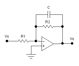
Figure 4
Low Pass Filter
2. ANALOG ACTIVE
HIGH-PASS FILTER
Design and
test a high-pass filter, Figure 5 with a high-frequency voltage gain of 14 dB
and a 3 dB corner frequency in the range of 50 Hz to 200 Hz. Do not use series and parallel capacitor
combinations or series and parallel resistor combinations. Use standard values from the parts cabinet
that yield a corner frequency and
voltage gain reasonably close to the specifications
Ø Experimentally verify your design and
simulation results.
Ø For verifying high-pass filter operation,
measure 20 log|A(jf)| and compare your results with the SPICE AC simulation
over a similar range.
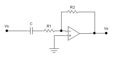
Figure 5 High Pass Filter
3. ANALOG ACTIVE BAND-PASS FILTER
Now cascade the
output of the HPF with the LPF (Figure 6) and note the band pass
characteristic. Measure 20 log|A(jf)| and compare your
results with the SPICE AC simulation over a similar range. The center of your filter design will peak
near 34 dB or about |50|. You will have to adjust your input level to
avoid clipping.
Figure 6 Band Pass Filter
4. WIEN BRIDGE
OSCILLATOR
So far, all of the
circuits we have studied employ negative feedback. The following circuit, Figure 7, employs positive feedback; and as mentioned
in class, an audio example of positive feedback
is the “howl” observed when the microphone and speaker are not placed well in
an auditorium and you have constructive (additive) signals. Construct the following circuit which is
similar to what is shown in Figure 12.43 on page 741 of the text. At first glance, the circuits look different
but they are the same. You are generating
a signal source, that is you are demonstrating the operation of an
oscillator. Observe that there is no
external signal generator!!!! Monitor vo(t)
using your oscilloscope. Observe there
is no input signal. This is called a Wien
Bridge Oscillator. Explain
why this is a useful circuit. (Note
depending upon the resistor tolerances and circuit losses, you may have to
increase your value of R2 somewhat; perhaps as high as 33 kΩ). Lead dress has an impact on the circuit
performance. Compare the observed
oscillating frequency of operation to
the equation,  and the voltage gain
required setting established by
and the voltage gain
required setting established by .The SPICE simulation approach is interesting and I will
demonstrate this when your group reaches that part of the lab. In a real circuit, an oscillator starts
through random noise which provides an initial signal with the correct phase
shift to obtain positive feedback .
To show this in a SPICE simulation, add an initial condition of several
tenths of a volt to each of the capacitors as an initial condition and then use
a transient analysis that extends for several periods of the expected frequency
output. The exponential signal growth is
kind of cool (at least I think so) to
watch during the simulation. The
simulation makes you a believer in exp(+αt) DFQ solution from EE 2006!
.The SPICE simulation approach is interesting and I will
demonstrate this when your group reaches that part of the lab. In a real circuit, an oscillator starts
through random noise which provides an initial signal with the correct phase
shift to obtain positive feedback .
To show this in a SPICE simulation, add an initial condition of several
tenths of a volt to each of the capacitors as an initial condition and then use
a transient analysis that extends for several periods of the expected frequency
output. The exponential signal growth is
kind of cool (at least I think so) to
watch during the simulation. The
simulation makes you a believer in exp(+αt) DFQ solution from EE 2006!

Figure
7 Wien Bridge Oscillator

Alternative definition for
mobility
And micrometer
$1200+ for a loaded iPhone
13Pro.
I wonder what the rumor
mills are speculation for the iPhone 99 ?
Maybe an inexpensive basic
model? Built in beverage dispenser?,
etc.

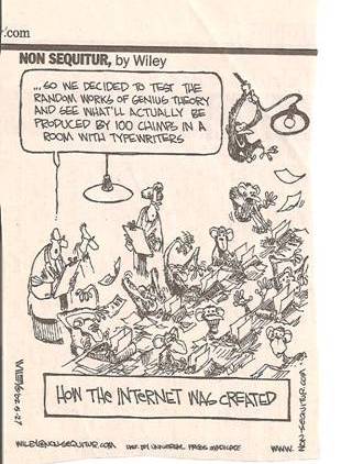
Do you believe this
explanation or the one claiming the WEB originated
as a spin-off of a U.S. Department of Defense ARPANET
project?
Time to start thinking about outside of EE technical electives registration for Spring
semester and next year.


Also think about a UROP.