EE 2212
Fall 2018
13 September 2018
Experiment 2: Basic Operational Amplifier
Circuits
Report Due: 20 September February
Note 1: I
will provide an overview of the op amp SPICE models at the beginning of the
laboratory. We will be discussing time
domain and frequency domain analysis.
Note 2: Your frequency-independent designs will be used as the basis for analog
active LPF, HPF, and Band-Pass filter designs in in Experiment 3, 20 September.
PURPOSE
To implement the designs of:
Ø Two
versions of an inverting operational amplifier (Figures 1 and 3)
Ø A
non-inverting operational amplifier
Ø A
cascade of an inverting and non-inverting amplifier.
GENERAL COMMENTS
Run the
SPICE time-domain simulation with a VSIN generator and the frequency-domain
simulation with a VAC generator. Use the μA741 model in the eval.slb library.
Print the waveforms of the inputs and outputs on the same set of axes.
You will need the following information from your SPICE simulations in order to
complete this lab:
Ø TRANSIENT analysis
for a sinusoidal input
Your hardware realizations designs must not
incorporate series and parallel resistors to meet the voltage gain specifications. It is more desirable to come close with
standard value components and use the exact measured numbers in your circuit
simulation.
PRELAB
Ø Specify
the component values
to meet the indicated specifications for Circuits 1 and 2 . You should
come to the lab with a list of the components you will need to meet the
specifications. You might refer to your EE 2006 notes and labs since you have
worked with op amps in that course.
The derivation, in
your notebook, of the voltage gain
Vo/Vs for Circuit 3
using summing point constraints. This is also a good exercise in
the use of nodal analysis. (R2, R3, R4 node)
PROCEDURE
Refer to the mA741
data sheet on the class WEB page uA741.pdf. Observe, you are using the 8-pin DIP
(Dual-Inline Package), second package style from
the top. This package is also sometimes called the
MINIDIP. Also note that the mA741 has certain requirements with respect to allowed resistance values
that includes all resistors in your
design must be greater than or equal to 2 kW. Do not include the 10 kW offset
voltage potentiometer.
Use ± 12 volts for the power
supplies. Verify that the polarities
are correct or ![MM900336554[1]](Experiment2BasicOpAmpCircuits_files/image002.gif) you will create a classic embarrassing odor
you will create a classic embarrassing odor![]()
![]() not correctable with Old
SPICE (pretty good pun!) body wash.
not correctable with Old
SPICE (pretty good pun!) body wash.
Your designs should be
supported analytically and by SPICE simulation results. You should record all key oscilloscope
waveforms on your flash drive
as support for your
laboratory report.
1. For Figure 1. Design and test an inverting amplifier with a
low-frequency voltage gain of 20 dB.
Ø Start
with a 1 kHz
sinusoidal input voltage. The input
voltage level is not critical as long as you do not observe clipping on your output
waveform.
Ø Experimentally
verify your design and simulation results in the time domain.
Ø Experimentally
determine the input signal level when “clipping” of the output
waveforms occurs.*
Ø Observe
the resultant transfer
characteristic. The transfer
characteristic is a plot of
Vout versus Vin. In order to see the transfer characteristic
on the oscilloscope, you will need to change the display to “XY” mode. Select the “Display” key and select “XY
Display” from the menu. Switch to
“Triggered XY” mode. You may use the
scale controls to adjust the axes accordingly.
Also verify your voltage gain and phase shift measurements using the
transfer characteristic. Note the
negative slope is indicative of the low frequency 180°of phase shift in an
inverting amplifier.
Ø Measure
and plot the voltage
gain in dB as a function of frequency,
and q(jf),
which is the phase shift as a function of frequency, through the amplifier
circuit, and compare your results with the SPICE AC simulation. Extend your measurements to a 10 kHz or so. Plot the results as you take your
measurements. Note that if the Greek
(Theta) q(jf)
printed out as q(jf), your WEB browser and/or word
processing program does not translate symbol font correctly.
*Go
slow in increasing the amplitude of Vs! Do not overdo the input voltage to
observe clipping because if your input becomes too large, you will damage the mA741.
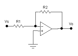
Figure 1 Inverting
Operational Amplifier Circuit
2. For Figure 2. Design and test a non- inverting amplifier
with a low-frequency voltage gain of 14 dB.
You are essentially repeating the procedure for
Figure 1.
Ø Start
with a 1 kHz
sinusoidal input voltage. The input
voltage level is not critical as long as you do not observe clipping on your output
waveform.
Ø Experimentally
verify your design and simulation results in the time domain.
Ø Experimentally
determine the input signal level when “clipping” of the output
waveforms occur.*
Ø Observe
the transfer
characteristic. The transfer
characteristic is a plot of
Vout versus Vin. In order to see the transfer characteristic
on the oscilloscope, you will need to change the display to “XY” mode. Select the “Display” key and select “XY
Display” from the menu. Switch to
“Triggered XY” mode. You may use the
scale controls to adjust the axes accordingly.
Also verify your voltage gain and phase shift measurements using the
transfer characteristic. Note the positive slope
indicative of the low frequency 0° of phase shift.
Ø Measure
and plot the voltage
gain in dB as a function of frequency,
and q(jf), which is the phase shift as a function of frequency,
through the amplifier circuit, and compare your results with the SPICE AC
simulation. Extend your measurements to
a 10 kHz or so. Plot the results as you
take your measurements.
*Go
slow in increasing the amplitude of Vs! Do not overdo the input voltage to
observe clipping because if your input becomes too large, you will damage the mA741.
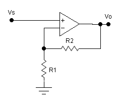
Figure 2 Non-Inverting
Operational Amplifier Circuit
3. Cascade
amplifier topology
Connect the input of Circuit 2 to the output of
Circuit 1 which results in a cascade amplifier configuration. Your cascade gain will be 20 dB + 14 dB = 34
db.
Ø Set
the input frequency to a 1 kHz sinusoidal input voltage. The input voltage level is not critical* as
long as you do not clip your output waveform. Note that the magnitude of your cascade gain
is about 50, i.e. 34 dB.
Ø Experimentally
verify your design and simulation results in the time domain.
Ø Measure
20 log|A(jf), the voltage gain in dB, and the phase, q(jf) and compare your
results with the SPICE AC simulation. Extend your measurements to 10 kHz or
so. Plot your results as you collect the
data.
Ø Observe
the transfer function and verify the voltage gain and low frequency phase shift
from the slope at 1 kHz.
*Note that your input
level will be much less than used for either circuits 1 or 2 since the cascade
gain is now 34 dB.
4. Another
Inverting Amplifier Configuration. Refer
to Figure 3.
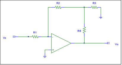
Figure 3 Another Inverting Operational Amplifier Circuit
Use all 10 kW
resistors. Verify experimentally and
using SPICE, the voltage gain at 1 kHz . Use both a time domain and transfer
characteristic representation of your work.
Frequency response measurements are not
Required Hint: The voltage gain should be -3 from your
PRELAB derivation.
Some suggestions for writing laboratory reports
although not part of our grading rubric.
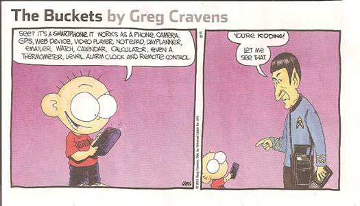
For
those of you who are “trekies” i.e. fans of the vintage Star Trek
television series (50+ years old) and have a “smartphone”. By the way, NETFLIX has all of the original
episodes which beats my pile of vintage VHS video cassettes I used to have of all
the episodes. I also noted an article on
CNN http://www.cnn.com/2014/09/03/tech/innovation/tricorder-x-prize-finalists/index.html
that I thought was interesting. And the
winner was https://www.nbcnews.com/mach/technology/these-er-docs-invented-real-star-trek-tricorder-n755631 An Apple Watch does a good job with heart
rate and the FITBIT has all sorts of options.
My
take on computer “customer service”. I
feel so honored that my call is important to them as I listen to their
so-called music.