EE 2212
Spring 2019
7 February 2019
Experiment 2: Frequency Domain Response for
Passive Circuits and Operational Amplifier Circuits
Report Due: 14 February in Lab
Note 1: I will discuss the implementation of AC SPICE
analysis in our lab introduction.
Note 2: I will provide an overview of the op amp SPICE
models also at the beginning of the laboratory.
Note 3: Your frequency-independent designs will be used as the basis for the analog
active LPF, HPF, and Band-Pass filter designs
in Experiment 3, 14 February
Note 4: Because we missed lab last Thursday, snow
day, I am combining elements of two lab experiments; consequently I am allowing
up to five additional pages to accommodate graphs besides the cover sheet
instead of three additional pages.
Note 5: EXCEL spread sheets are a good way to collect
and display your data. EXCEL is resident
on the lab computers and available through ITSS for your computers.
1. Construct
the following two circuits on your prototype board. Observe that the circuits
are duals of each other.
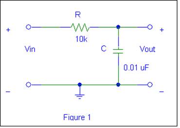
Frequency Domain Response Using Figure 1 (Low-Pass Filter)
You will now demonstrate analog filters. Filters, whether analog or digital, are very
important components in most electronic systems
The circuit in Figure 1 is a
basic single-pole analog, passive, low-pass filter (LPF). This LPF function can
be observed by applying a constant-amplitude
(i.e. 1volt peak amplitude input sinusoid and
varying the frequency from 100 Hz to > 20 kHz.
Ø Measure, record and plot the voltage gain in
dB and phase shift as a function of frequency (on a log scale). This is often called a Bode Plot. You may have seen similar plots for some of
your audio equipment. Start at 100 Hz
and end at a few tens of kHz. Measure
the – 3 dB corner frequency of the filter, and the phase shift at that
frequency. (Note that –3 dB corresponds
to 70.7% of the low-frequency gain).
Again, you can obtain phase directly from the oscilloscope “MEASURE”
menu and visually verify by looking at the waveforms. Compare these measurements with theoretical
and PSPICE values. Many of these measurements can be done by using soft key
settings within the oscilloscope “MEASURE” menu.
Ø Compare your data to SPICE AC analysis plot.
FREQUENCY
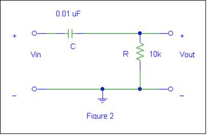
DOMAIN RESPONSE Of Figure 2 (High Pass Filter)
The circuit in Figure 2 is also
a basic single-pole passive high-pass filter. To see this, observe the
amplitude of the output as the frequency is varied from >20 kHz down to 100 Hz. You will
need to use a 1 volt peak- amplitude input sinusoid.
Ø Measure, record and plot the voltage gain in
dB and phase shift as a function of frequency (on a log scale). Start at a few tens of kHz and end at 100
Hz. Measure the – 3 dB corner frequency
of the filter, and the phase shift at that frequency. (Note that –3 dB corresponds to 70.7% of the
high-frequency gain). Again, you can
obtain phase directly from the “MEASURE” menu and visually verify by looking at
the waveforms. Compare these
measurements with theoretical and PSPICE values. Many of these measurements can
be done by using soft key settings within the oscilloscope “MEASURE” menu.
Ø Compare your data to SPICE AC analysis plot.
Ø Note that the -3dB frequency is the same for
both the LPF and HPF since R and C are the same values.
3. To
implement the designs of:
Ø An
inverting operational amplifier, Figure
3
Ø A
non-inverting operational amplifier, Figure 4
Note 1: Run the SPICE
time-domain simulation with a VSIN generator and the frequency-domain simulation
with a VAC generator. Use the μA741
model in the eval.slb library. Print the waveforms of the inputs and outputs
on the same set of axes. You will need the following information from your
SPICE simulations in order to complete this lab:
Ø TRANSIENT analysis
for a sinusoidal input
Ø Your
hardware realizations designs must not incorporate series and parallel
resistors to meet the voltage gain specifications. It is more desirable to come close with
standard value components and use the exact measured numbers in your circuit
simulation.
Ø Specify
the component values
to meet the indicated specifications for Circuits 3 and 4 . You
should come to the lab with a list of the components you will need to meet the specifications.
You might refer to your EE 2006 notes and labs since you have worked with op
amps in that course. All resistor values
must be 2 kΩ or larger for the μA741
PROCEDURE
Ø
Refer to the mA741 data
sheet on the class WEB page uA741.pdf. Observe, you are using the 8-pin DIP
(Dual-Inline Package), second package style from
the top. This package is also sometimes called the
MINIDIP. Also note that the mA741 has certain requirements with respect to allowed resistance values that
includes all resistors in your design
must be greater than or equal to 2 kW. Do not include the 10 kW offset
voltage potentiometer in your design.
Ø
Use ± 12 volts
for the power supplies. Verify that the
polarities are correct or ![MM900336554[1]](Experiment2FrequencyDomainResponseForPassiveCircuitsAndOperationalAmplifierCircuits_files/image006.gif) you will create a classic embarrassing odor
you will create a classic embarrassing odor![]()
![]() not correctable with Old SPICE (pretty good
pun!) body wash.
not correctable with Old SPICE (pretty good
pun!) body wash.
Ø Your designs should be supported analytically and by SPICE
simulation results. You should record
all key oscilloscope waveforms on your flash drive as support for your laboratory report.
1. For Figure 1. Design and test an inverting amplifier with a
low-frequency voltage gain of 20 dB.
Ø Start
with a 1 kHz
sinusoidal input voltage. The input
voltage level is not critical as long as you do not observe clipping on your output
waveform.
Ø Experimentally
verify your design and simulation results in the time domain.
Ø Experimentally
determine the input signal level when “clipping” of the output
waveforms occurs.*
Ø Observe
the resultant transfer
characteristic. The transfer
characteristic is a plot of
Vout versus Vin. In order to see the transfer characteristic
on the oscilloscope, you will need to change the display to “XY” mode. Select the “Display” key and select “XY
Display” from the menu. Switch to
“Triggered XY” mode. You may use the
scale controls to adjust the axes accordingly.
Also verify your voltage gain and phase shift measurements using the
transfer characteristic. Note the
negative slope is indicative of the low frequency 180°of phase shift in an
inverting amplifier.
Ø Measure
and plot the voltage
gain in dB as a function of frequency,
and q(jf),
which is the phase shift as a function of frequency, and compare your results
with the SPICE AC simulation. Extend your
measurements to 10 kHz or so. Plot the
results as you take your measurements.
Note that if the Greek (Theta) q(jf) printed out as q(jf), your
WEB browser and/or word processing program does not translate symbol font
correctly.
*Go
slow in increasing the amplitude of Vs! Do not overdo the input voltage to
observe clipping because if your input becomes too large, you will damage the mA741.
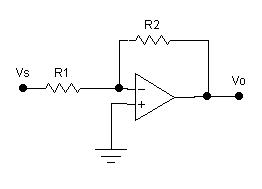
Figure 3 Inverting
Operational Amplifier Circuit
2. For Figure 2. Design and test a non- inverting amplifier
with a low-frequency voltage gain of 14 dB.
You are essentially repeating the procedure for
Figure 1.
Ø Start
with a 1 kHz
sinusoidal input voltage. The input
voltage level is not critical as long as you do not observe clipping on your output
waveform.
Ø Experimentally
verify your design and simulation results in the time domain.
Ø Experimentally
determine the input signal level when “clipping” of the output
waveforms occur.*
Ø Observe
the transfer
characteristic. The transfer
characteristic is a plot of
Vout versus Vin. In order to see the transfer characteristic
on the oscilloscope, you will need to change the display to “XY” mode. Select the “Display” key and select “XY
Display” from the menu. Switch to
“Triggered XY” mode. You may use the
scale controls to adjust the axes accordingly.
Also verify your voltage gain and phase shift measurements using the
transfer characteristic. Note the positive slope
indicative of the low frequency 0° of phase shift.
Ø Measure
and plot the voltage
gain in dB as a function of frequency
and q(jf), which is the phase shift as a function of frequency, and
compare your results with the SPICE AC simulation. Extend your measurements to a 10 kHz or
so. Plot the results as you take your
measurements.
*Go
slow in increasing the amplitude of Vs! Do not overdo the input voltage to
observe clipping because if your input becomes too large, you will damage the mA741.
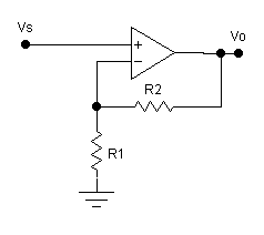
Figure 4 Non-Inverting
Operational Amplifier Circuit
Some suggestions for writing laboratory reports
although not part of our grading rubric.

For
those of you who are “trekies” i.e. fans of the vintage Star Trek
television series (50+ years old) and have a “smartphone”. By the way, NETFLIX has all of the original
episodes which beats my pile of vintage VHS video cassettes I used to have of
all the episodes. I also noted an
article on CNN http://www.cnn.com/2014/09/03/tech/innovation/tricorder-x-prize-finalists/index.html
that I thought was interesting. And the
winner was https://www.nbcnews.com/mach/technology/these-er-docs-invented-real-star-trek-tricorder-n755631 An Apple Watch 4 does a good job with
heart rate and EKG, and the FITBIT has all sorts of options.
My
take on computer “customer service”. I
feel so “honored” that my call is important to them as I listen to their
so-called elevator music.