EE
2212
EXPERIMENT
5
15
October 2020
The Half Wave Rectifier and Precision Rectification
Lab
Report Due: Thursday, 22 October
PURPOSE
Ø
Use
of the HANTEK 2D42 DMM to Test Diodes
Ø
Implement
designs of the half wave rectifier circuit and measure time domain
characteristics and the transfer characteristic, vo(t) vs. vs(t).
Ø
Measure
and compute ripple voltage as a percentage and as an rms
value. Compare individual diode results
and circuit results using SPICE simulations.
COMPONENTS
Ø
1N4002
or the 1N4001 Diode (Use the 1N4002 diode model in the SPICE library)
Ø
2 kΩ and 1 kΩ
resistors
Ø
0.1
μF, 1μF, and 10μF capacitors Actual values not critical since you
are just showing the “filtering/smoothing” effect to minimize ripple
voltage.
PROCEDURE
Ø
You can use the HANTEK 2D42 DMM to measure the
functionality of a junction; specifically the 1N4002.
·
Turn
on the HANTEK and press the “DMM” key.
·
Toggle
the F4 menu to the 4th screen, 4/4
·
Toggle
F1 to highlight the diode symbol
·
Connect
the DMM leads (Forward and Reverse) and verify forward and reverse bias diode operation
Ø Examine the model characteristics for the 1N4002
PSPICE, which can be
found by selecting the device and then Edit_Model…_Edit
Instance Model (Text)… You will use this
information for comparing to your measurements.
Half-Wave
Rectifier
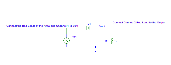
Ø Refer to Figure 1. Your signal source to a 2.5 volt zero-to-peak 1000 Hz sinusoid.
·
The
HANTEK 2D42 AWG (Signal Generator) has a limited range of 5 volts peak-to-peak
or 2.5 volts which does limit the types of experiments we can perform
·
Set
up the AWG leads as shown in Figure 1.
Be sure the AWG is on “Green” icon is on.
·
Toggle
F4 to Screen 1. Then toggle F1 to Sine;
toggle F2 to set frequency of 1 kHz using the arrow keys
·
Toggle
F4 to Screen 2 and then toggle F2 and adjust offset to 0 volts using the
left-right arrow keys.
Ø Perform a SPICE transient analysis
simulation and observe the
half-wave rectified output like we did in a class demonstration. Refer to PowerPoint class notes. Also note the effect
of the diode offset voltage when you compare the input and output
waveforms. Observe and plot Vout(t)
and the transfer characteristic, Vo vs Vs(t).
· To obtain the transfer characteristic, Press
the “Time” button and toggle to X-Y from Y-T screen
Ø Experimentally observe the operation on the
oscilloscope in both the time domain and as a transfer function.
Ø Now we want to “smooth out” the pulsating DC by
using capacitors. Place a C across the
1 kΩ resistor.
Use three values of C to illustrate the change in the ripple voltage by measuring Vout(t). Explain
the differences in these
measurements and explain what these measurements are
illustrating. Use your diode model and
check your lab measurements using SPICE.
Observe that ripple voltage is defined as either the (DV/Vpeak) x 100% or as (Vrms or as Vrms of the output
voltage/Vpeak)x 100% )x 100%. Watch your polarity on the electrolytic
capacitors or else ![MM900336554[1]](Experiment5DiodeParameterExtractionAndHalfWaveRectifierRev1_files/image003.gif) Also, since electrolytic
capacitors have
a broad tolerance, their values must be checked on the capacitance meter to obtain accurate results.
Also, since electrolytic
capacitors have
a broad tolerance, their values must be checked on the capacitance meter to obtain accurate results.
PRECISION
RECTIFICATION-DIGITAL SIGNAL PROCESSING FUNCTION (DSP)
Ø Precision
rectification is used in DSP (Digital Signal Processing) applications where the
“switch” and absolute value function needs to be implemented but there must be
a minimization of the effect of the diode forward voltage. Can we design a circuit that minimizes the 0.7 volt forward voltage drop? Of course
the answer is yes or why would we spend the time in the lab demonstrating this!
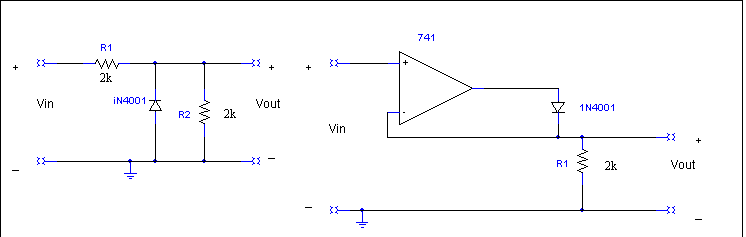
Ø Measure the transfer
characteristic, Vout as a function of Vin of the circuit
shown in Figure 2(a). Use either the
1N4001 or 1N4002 diodes. Pay particular attention to the effect of the
diode offset voltage when you measure the transfer characteristic.. Now construct the
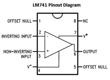
circuit shown in Figure 2(b). Use ±9 volts (Two battery
packs) for the mA 741 operational
amplifier. Measure the transfer
characteristic and compare to the results in Figure 2(a). Justify the term “precision rectification”
when applied to the circuit in Figure 2(b).
Refer to Section 12.8 of the text, page 745, Figure 12.51 for additional
information. Simulate in SPICE showing
the transfer characteristic.
Again, AWG output red lead and Ch. 1 red lead connect to Vin and the Channel 2 Red lead connects to Vout.
As with the half-wave rectifier, you can toggle between Y-T and X-Y
for time domain and transfer characteristic respectively.
Ø
=
Figure
2 (a) and Figure 2 (b)
More Good Stuff-The 10 Commandments (Sort of archaic prose but
fun). From an anonymous posting om the side of a file cabinet in an unnamed industrial
laboratory.