EE 2212
EXPERIMENT 5
27 February 2020
Full Wave Bridge Rectifier and Precision
Rectification Signal Processing Function
Diode-Bridge Full-Wave
Rectifier
Ø
Construct
the circuit shown in Figure 1. Note that
to provide a floating input from the signal generator which has one side grounded , we will use a transformer to provide
isolation. This is a common design
practice. There could be two styles of transformers in the bin. One plugs directly into the circuit board;
note the “P” stands for primary. The
second type has colored leads. Both are
essentially the same for our purposes.
Review transformer operation as discussed in our class a couple of weeks
ago. For this lab, turns ratio is
essentially 1:1.
Ø
Use
either the 1N4001 or 1N4002 diodes. For
our purposes, both have essentially the same specifications.
Ø
Do
not monitor the input of the bridge with the oscilloscope because you will
automatically ground (that is short circuit) one side of the circuit. Monitor
the input on the signal generator side of the circuit. (Brown and blue
transformer primary winding).
Ø
Also
observe how this floating input was modeled in SPICE. Refer to the SPICE demo in class from two
weeks ago. Observe that we did not use
a transformer in SPICE but connected a VSIN generator between the yellow wire
node and the green wire node. Use a
transient analysis.
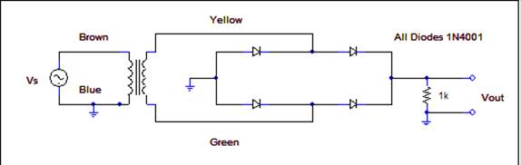
Figure 1 Full-Wave Bridge Rectifier
Ø Start by setting the input Vs as a 10 volt
zero-to-peak 100 Hz sinusoid. Same input
as we used for the half-wave rectifier in Experiment 4. Observe and plot Vo(t)
and the transfer characteristic, Vo vs Vs. Explain why this circuit would function as an
“absolute value” extraction function circuit as well as a rectifier.
Ø
Now
use a few values
of C from 1μF to 100 μF across the 1 kΩ
resistor to illustrate and measure the change in ripple voltages by measuring
Vo(t). Use the oscilloscope to measure the rms
voltage of the output using dc and ac coupling.
Ø
Compare
your full-wave rectifier results with SPICE simulations and the half-wave rectifier circuits
studied in Experiment 4.
PRECISION RECTIFICATION-DIGITAL SIGNAL PROCESSING FUNCTION
(DSP)
Precision
rectification is used in DSP (Digital Signal Processing) applications where the
“switch” and absolute value function needs to be implemented but there must be
a minimization of the effect of the diode forward voltage. Can we design a circuit that minimizes the
0.7 volt forward voltage drop? Of course the answer is yes or why would we
spend the time in the lab demonstrating this!
Measure
the transfer characteristic, Vout as a function of Vin of the circuit
shown in Figure 2(a). Pay particular
attention to the effect of the diode offset voltage. Now construct the circuit shown in Figure
2(b). Use ±12 volts
for the mA 741
operational amplifier. Measure the
transfer characteristic and compare to the results in Figure 2(a). Justify the term “precision rectification”
when applied to the circuit in Figure 2(b).
Refer to Section 12.8 of the text, page 745, Figure 12.51 for additional
information. Simulate in SPICE showing
the transfer characteristic.
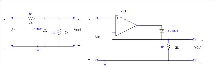
Figure 2 (a) and Figure 2(b)
More Good Stuff-The 10
Commandments (Sort of archaic prose but fun)