EE
2212
Experiment 7
11 November 2021
THREE MOSFET AMPLIFIER CIRCUITS
Study
transfer
characteristics of three circuits and compare with the SPICE simulations
Ø NMOS Inverter with a Resistive Load
Ø NMOS Inverter with an Active Load
Ø CMOS Inverter
COMPONENTS
Ø CD4007 MOSFET array
Ø 3.3 kW resistor
PRELAB
The device you will use
throughout this experiment is a CD4007B/UB Transistor array. It contains three
N-channel and three P-channel devices connected as shown. Detailed schematic diagrams and pinouts are
available on the data sheet and also given below. Please use care when working with these
chips. They are very susceptible to excessive voltage and ESD (Electro-Static Damage). Do not exceed the experiment settings in an
attempt to make your experiment work. The pin configuration is given in
Figure 7.1. Note that you will be using
the CD4007B which have a lower maximum voltage rating than the CD4007UB. The diagrams are the same for both the “B”
and “UB” suffix devices. Avoid exposing
the chip to ESD (electrostatic damage).
This time of the year often has low relative humidity which make ESD more of an issue. Do not exceed the VDD maximums!!!
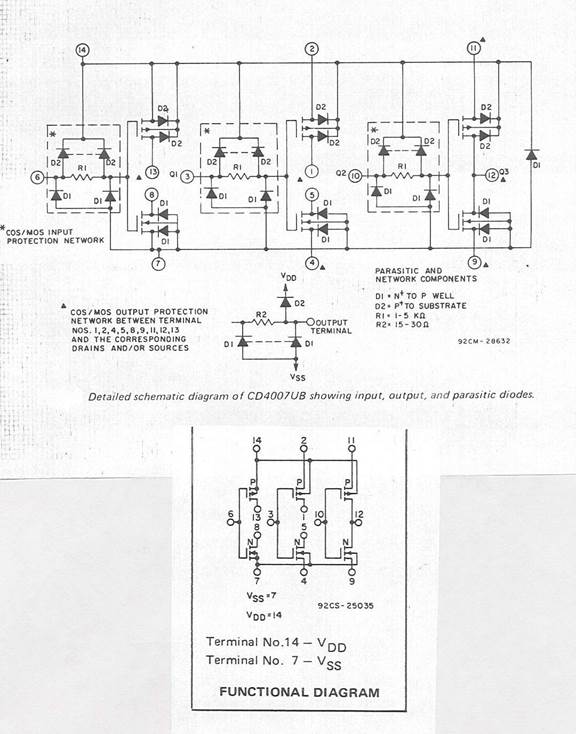
Figure 7.1 Pin Configuration of CD4007.
Warning: Pin 14 should always be connected to the
most positive dc voltage in the circuit.
Pin 7 will always be connected to the most negative dc voltage in the
circuit which is system ground in this case.
(or else ![MCBS00726_0000[1]](./Experiment7ThreeMOSAmplifierCircuits_files/image020.gif) )!!!
)!!!
PROCEDURE
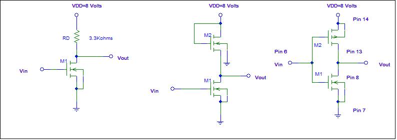
INVERTER CIRCUITS
Refer to the three circuit
diagrams in Figures 7.2, 7.3, and 7.4. All will operate with a VDD = +8 volt
power supply. VSS = 0 Volts. Remember Pin 14 should always be connected to
the most positive dc voltage in the circuit.
Pin 7 will always be connected to the most negative dc voltage in the circuit which is
ground for these circuits..
You will need to arrange for an
offset voltage (4 volts) from the signal generator so that Vin
does not go below zero volts.
To standardize on the SPICE
simulations, use VTO = 2 volts for the NMOS and VTO = -2 volts for the PMOS; λ= 0.02 volts-1, and KP
= 50E-3. The default KP does not do a
good job in modeling the CD4007 devices which means the circuits will not
exhibit the measured
voltage gain. Use default values for all
other SPICE model parameters.
1. Set up the NMOS Inverter with a Resistive
Load as shown in Figure 7.2. Use the NMOS FET connected to CD4007 M1 Pins 6, 7,
and 8. Before connecting your function
generator to the circuit input, adjust it for a 0-8 V sinusoidal waveform at a frequency of 1 kHz. You
will need to use the dc-offset control on your function generator to do this.
That is an 8 volt peak-to-peak sinusoid with a 4 volt dc offset. Therefore, the input voltage will go from 0 to + 8
volts. Plot the transfer characteristic,
that is Vout versus Vin. Connect the input and output
to the horizontal and vertical inputs (respectively) of your oscilloscope set
to the x-y mode. This arrangement allows you to display the transfer
characteristic of the circuit. Identify
the saturation, ohmic, and cutoff regions of
operation. Suggest a Q-point to obtain the largest small-signal voltage gain (steepest
slope). Verify your experimental results with a SPICE simulation. Important to observe that you will need to
provide a dc offset from the signal generator.
2. Set up the actively-loaded NMOS Inverter as
shown in Figure 7.3. Use CD4007 M1 Pins
6, 7, and 8 and M2 Pins 3, 4, and 5.
Before connecting your function generator to the circuit input, adjust
it for a 0-8 V sinusoid at a frequency of 1 kHz. You will need to use the
dc-offset control on your function generator to do this. That is an 8 volt
peak-to-peak sinusoid added to a 4 volt dc offset. Connect the input and output to the
horizontal and vertical inputs (respectively) of your oscilloscope set to the
x-y mode. This arrangement allows you to display the transfer characteristic of
the circuit. Plot the transfer
characteristic. Identify the saturation, ohmic, and
cutoff regions of operation for each FET. Suggest a Q-point to obtain the
largest small-signal voltage gain. Compare your results with the
resistively-loaded circuit. Observe that you will need to provide a dc offset
from the signal generator.
![]()
Figure 7.2 NMOS Inverter Resistive Load Figure 7.3 NMOS Inverter Active Load Figure 7.4 CMOS Inverter
3.
Connect the CMOS inverter circuit of Figure
7.4. with the CD4007 pins shown. You can
also use the CMOS inverter FETS connected using Pins 9, 10, 11, and 12. Connect the input and output to the
horizontal and vertical inputs (respectively) of your oscilloscope set to the
x-y mode. This arrangement allows you to display the transfer characteristic of
the circuit. Before connecting your function generator to the circuit input,
adjust it for a 0-8 V sinusoid at a frequency of 1 kHz. You will need to use the
dc-offset control on your function generator to do this. That is an 8 volt peak-to-peak sinusoid with a 4 volt dc offset. Observe and sketch the transfer
characteristic, recording all critical values of voltage. Your report should include a PSPICE simulation
of this circuit using NMOS and PMOS models.
Compare to the 4007 curves on the data sheets.
A few more items to think about.
Compare the static power dissipation of the three circuits CMOS Inverter, NMOS Inverter
with a resistive load, NMOS inverter with an active load when operated as
switches/inverters as opposed to amplifier operation.
These Cartoons Represent EE at
its Finest!


![]()