EE
2212
PROBLEM
SET 6
S.
G. Burns
Due: Wednesday, 17 March 2021
NOTE 1: Table 4.6
on Page 203 provides useful generic FET specifications information. If these data are not provided in any of the
Chapter 4 text problems, use information in Table 4.6. Also the inside of the front cover has all
sorts of useful data. Just
below Table 4.6 on Page 203, you will also
find some key constants; also on the inside of the front cover.
NOTE 2: I also want to call your attention to the
following link from our WEB page
FETNMOSSummary.tif FETPMOSSummary.jpeg
NOTE 3: Be sure your WEB browser
displays symbol font correctly.
1. Text Problem 4.1 (Look at Figure 4.2 for
guidance) and
Text Problem 4.2 as a combination. For
Text 4.2 observe that you are computing Cox, capacitance per unit area. Watch your units. Usually farads/cm2 (cgs system) is preferred for the capacitance per unit area
units. When the text and in the industry talks about an MOS capacitor, they are
usually referring to capacitance/unit area. The total capacitance can then be
scaled by multiplying by
(W x L). Refer to Monday,
5 and 10 March PPTs. This idea of
scaling is a very important VLSI design concept. The parallel plate basic capacitor model
works well! We will also soon observe
how this plays into imaging and display applications.
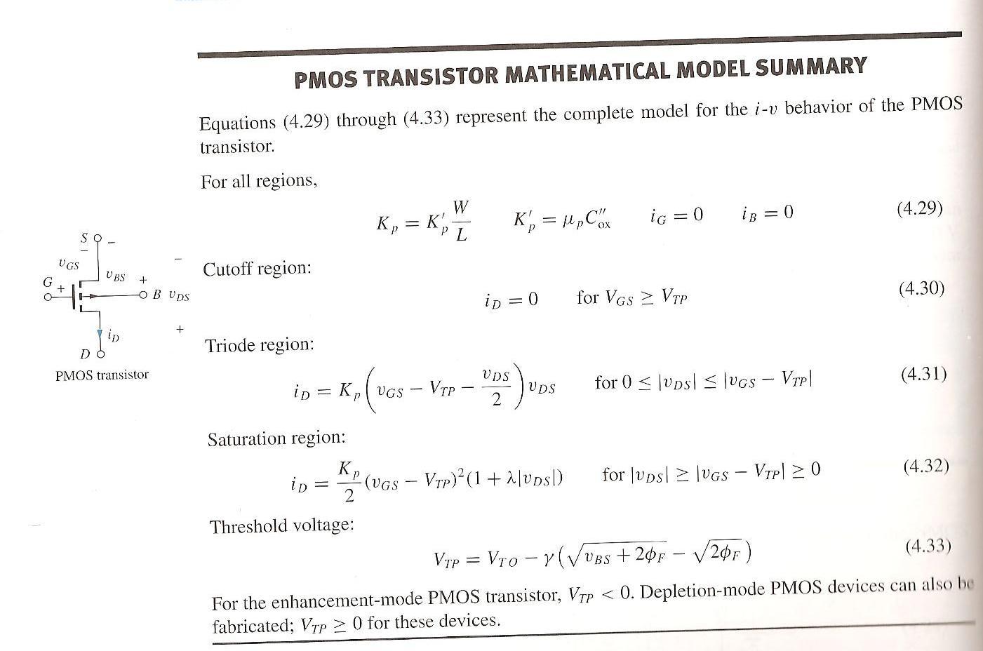
2. Text 4.4 and 4.8 for NMOS and Text 4.47
for PMOS. Plug and Chug. Some additional basic calculations to provide
experience in units and nomenclature.
Organize your results in a table.
Page 160 (NMOS) and 161 (PMOS) has a table defining the relationships
for key FET model parameters. Refer to
the WEB links in Note 2.
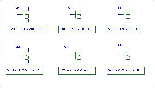
3.
Extracted from an old quiz. Regions of operation are very important in
circuit design using MOSFETS. For the
indicated bias conditions, state whether the FET is operating in the OHMIC
(TRIODE) region, SATURATION region, or CUTOFF region. Explain your reasoning. Assume that |VT | = 2 volts for both the
NMOS and PMOS enhancement mode transistors.
Arrow in for NMOS; arrow out for PMOS!!! M1 __________ M2 __________ M3
__________
M4 __________ M5
__________ M6 __________
4. Versions
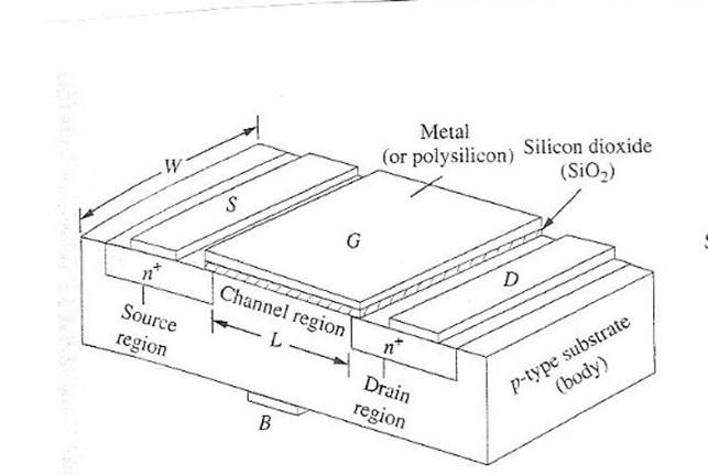
of this problem have also been extracted from old quizzes. Refer to the sketch of an n-channel
enhancement-mode MOSFET fabricated in silicon. Assume room temperature
operation. Also assume
l = 0. Units are important. (a) through (d) are
a modest sample of what could asked about the operation and physics of the NMOS and PMOS on a quiz.
(Subtle Hint!!!)
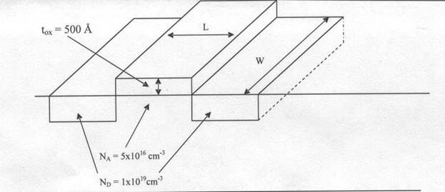
![]()
(a)
Compute
a value for Cox .
(b)
Compute
a value for the threshold voltage, Vt
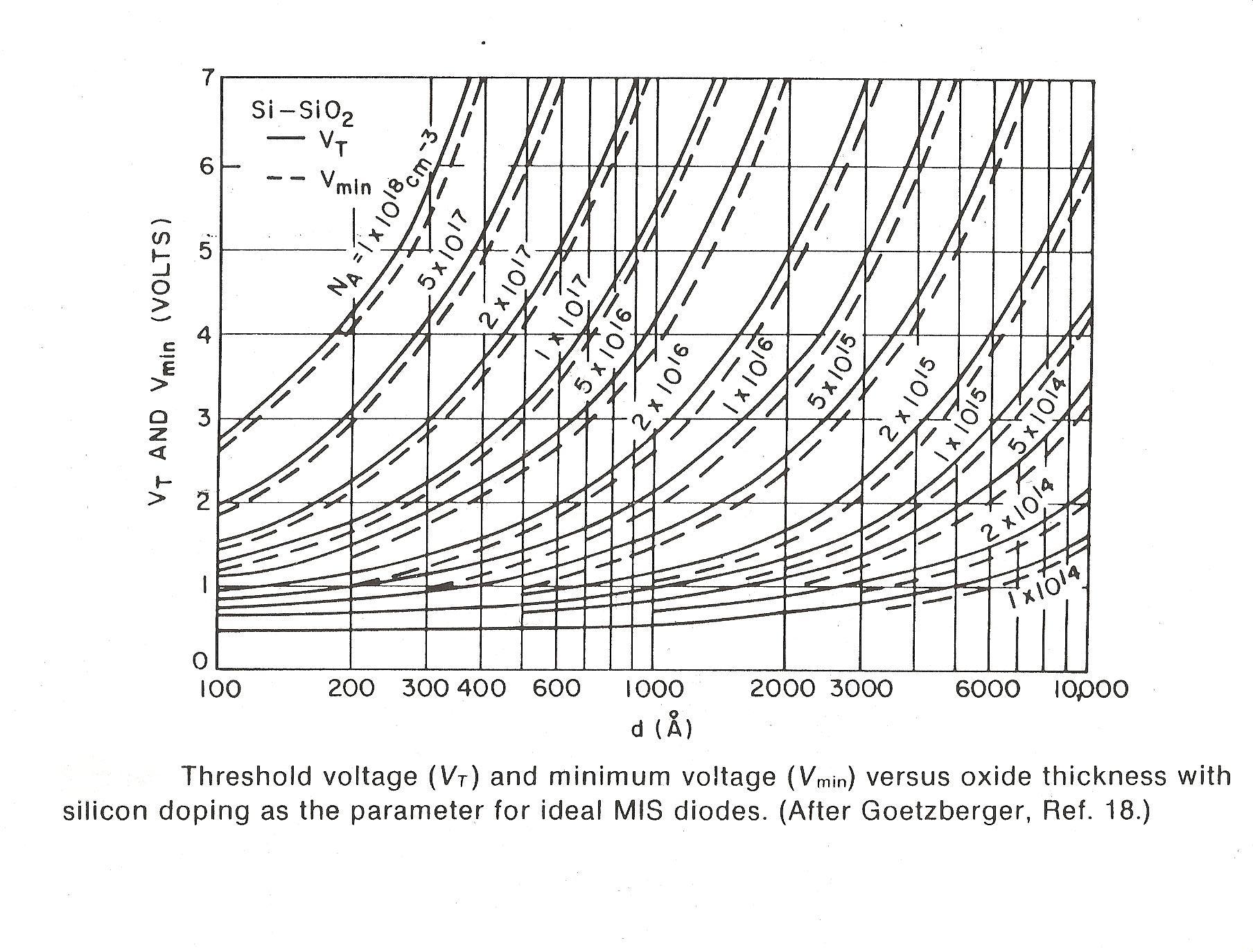
using the threshold voltage graph posted on the WEB page. ThresholdVoltageChart.JPG Assume
W/L = 10 and make reasonable assumptions and/or use values from Table 4.6 for
any other physical parameters you
may need. Compute values for “k” and
“KP” and then use your results from this
part and Parts (a) and (b) to generate a Shichmann-Hodges
Level 1 model equation.
(c)Using your calculated results from Part (c),
sketch and numerically label the iD versus
vDS as a function
of VGS curves. Label the
Saturation, Cutoff, and Ohmic (Triode) regions.
5.
Another sample quiz problem relating to FET
properties. Figure from the text.
(a) If
the substrate doping is NA
= 2 x 1017 cm-3 the inverted channel charge carriers
are (HOLES, ELECTRONS, BOTH HOLES AND ELECTRONS,
NEUTRONS, PHOTONS) and if the substrate doping is changed to be ND = 2 x 1017 cm-3,
the inverted channel charge carriers are (HOLES, ELECTRONS, BOTH HOLES AND
ELECTRONS, NEUTRONS, PHOTONS)
(b) The
input resistance looking in to the gate terminal is (CLOSE TO ZERO, GOVERNED BY
R=V/I, ESSENTIALLY INFINITE)
consequently the gate current IG is
(CLOSE TO ZERO, GOVERNED BY R=V/I, ESSENTIALLY INFINITE) Circle your
choices.
(c) Assume
tox = 200 Å and the substrate doping is NA =
2 x 1017 cm-3 Find
a value for the threshold voltage, VT from the curves.
(d) Again
assume tox = 200 Å and W= 0.01 μm and L = 20 nm.
Compute Cox and C.
This is what
we use for blocking dc and passing ac in many discrete device amplifier
circuits. Synonymous with coupling
capacitor. Also a dc blocking capacitor
is employed in your oscilloscope when switching to AC input using the soft
keys. Your HANTEK DMM with allow you switch coupling by toggling
the F4 button to screen 3; then F1 to yield AC volts. button. This function is the rms
value of the ac waveform.
Consider the signal swing around the Q-Point which established the
dynamic range of a circuit
which we will use in amplifier design

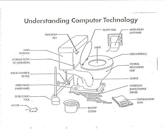
Even though
most of you are EE students, there is some information you can use from CS
I. Of course, you can always dive deeper
into CS but it messy in more ways than one, refer to the figure. I don’t know if this diagram is covered in
more advanced CS courses if you decide to work on a CprE Minor. Can you tell that I am a hardware guy!