EE
2212
PROBLEM
SET 7
S.
G. Burns
Due: Friday, 26 March 2021
Revised
with corrected dates for extra credit project.
EXTRA CREDIT OPPORTUNITY
Up to 30 Points added to your
end-of-the-semester Quiz Point Total. How do you earn this? I want
circuit diagrams and specifications for power amplifiers and related
equipment that you may have for some of your “stuff” and is usable, that is,
supports ZOOM in-class discussions when we get to power amplifiers
towards the end of the semester. Information such as circuit diagrams,
specifications for your sound systems, guitar
amps, car stereos, powered sub-woofers, associated power supplies, speaker
systems, etc. I define power loosely in that information on your portable
electronics such as wireless earbuds, smart phones, tablets, etc. also is
interesting to me and appropriate for class discussion. Homebrew projects
in these categories
are appropriate. I would
like to borrow the material to supplement our class discussions on power
amplifier circuits. Do not
just go to the WEB for information that doesn’t relate directly to stuff
you or your parents have. Hard Deadline for
receipt of materials is to be sent to me as an e-mail attachment (PPT or PDF)
by Wednesday, 14 April, 4 pm. Earlier is better so I can do a decent
scheduling job.! Be sure your name is in the submitted
materials. I will award up to 30 points based upon relevance and
class usability and you describing the item and
technical information to the class. Your
3-5 minute presentation via a ZOOM share will be scheduled for Wednesday
or Friday (21 or 23 April). Feel free if to discuss what you have with me if you have
questions. The meaner and badder stuff, the better.
The following problems provide practice in working with
small-signal models. Use the basic voltage-controlled current generator FET
small-signal model with λ (Lambda) =0.
In addition to answering the text questions, you are to draw and label
the resultant small-signal model circuit diagrams. Express your derivations symbolically; that
is no calculations are required. These problems also will familiarize you
with the text FET symbol notation variations.
It is important that you label circuit nodes carefully.
1. Draw the small-signal model for Figure
P13.5. After you have obtained the
small-signal model, derive an equation for the voltage gain defined by av
= vo/vi.
Observe that no numerical calculations
are required. Note that this circuit
uses an NMOS. This circuit is a
common-source.
2. Draw the small-signal model for Figure
P13.8. After you have obtained the
small-signal model, derive an equation for the voltage gain defined by av
= vo/vi.
Observe that no numerical calculations are required. Note that this circuit uses a PMOS. This circuit is a common-source.
3. Draw the small-signal model for Figure P13.9. After you have obtained the small-signal
model, derive an equation for the voltage gain defined
by av = vo/vi. Observe that no numerical calculations are
required. Note that this circuit uses an
NMOS. The circuit
is a common-gate.
4.
Small-Signal Model derivation for a cascade amplifier excerpted from an old quiz.
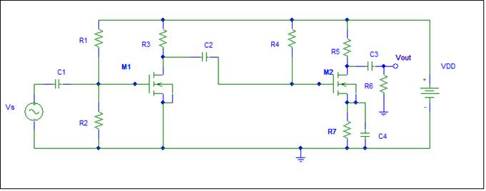
(a) Sketch and label a small-signal model for
this circuit which consists of two Common Source amplifiers in a cascade
configuration. Assume all capacitors are
large at the frequency of interest . Your model should be complete and
well-labeled. Assume λ= 0.
(b) Derive an expression for the voltage gain defined by Av = Vout/Vs . Observe no
numerical calculations are required.
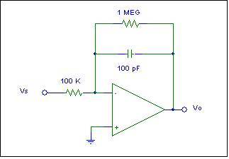
5. Synthesize a Resistor With A Switched Capacitor Circuit
Design a switched capacitor circuit that could be used to
synthesize a 10
kW resistor where the high
frequency band limit, of any signals
passing the equivalent synthesized
resistor, is in the range expected from
your audio band-limited smart phone. I
will accept any reasonable number for what you consider the highest frequency
for speech one could expect from your smart phone .
Your design should include:
· Well-labeled circuit diagram
· Design equations with key component values and an
appropriate clock frequency.
· Clock waveforms .
6. Switched Capacitor Low Pass Filter Design (excerpted
from an old quiz)
Use the basic concepts from the equivalent
resistor design discussed in class , design a switched
capacitor LPF that replaces the analog LPF; a topology we studied extensively
the first couple of weeks of the semester.
Design this circuit as a switched capacitor low-pass filter.
Your design should include:
· Well-labeled
circuit diagram.
· No
resistors-That is replace the two resistors with two switched capacitors and
four FETs. Your design should include appropriate W/L ratios for the four
FETs. An appropriate clock frequency for
operation at input signal frequencies to 5 kHz.
· Key
clock waveforms with the correct phasing for the four FETs illustrating the
operation.
It’s
all Greek to me
Alternate
definition for dynamic range.
Registration for your Fall
2021 classes is coming up soon!!! The following are dedicated to those of you
wanting to register for your breadth technical
elective.


For Those of You Planning to take Electromagnetics
(EE 3445)
And We Don’t Want To Forget the CprE/CS Minor
To Support the Energy Engineering Minor
And Also Consider the Math Minor

And there is always a UROP and Senior
Design!
