ECE 2212
Spring 2012
20 September 2012
Experiment 2: Operational Amplifier
Circuits 1
NOTE: I will be checking during your
that you are using a notebook as discussed earlier this semester. All information for Experiment 1 as well as
any pre-lab for this experiment must be in a patent acceptable notebook.
PURPOSE
Ø
To implement the
designs of inverting and non-inverting amplifiers using an operational
amplifier.
Ø
To modify the
SPICE frequency-independent model to simulate the measured frequency response
of the inverting operational amplifier
configuration.
Ø
To compare the
SPICE model discussed in class with the SPICE Schematic capture library model
which will include frequency effects.
PRELAB
Design the circuits to
meet the indicated specifications. You should come to the lab with a list of
the components you will need to meet the specifications. You might refer to
your ECE 2006 notes and labs since many of you have worked with op amps in that
course. Write and run SPICE time and
frequency domain programs for both circuits.
Use the .LIB 741 model if you have it in your version of SPICE and use
the linear model presented in class or the generic “op amp” in the .LIB
file. Print the waveforms of the inputs
and outputs on the same set of axes. You will need the following information
from your SPICE program in order to complete this lab:
Ø
3 dB BW, key
amplitudes, and times
Ø
.AC analysis of
frequency and phase
Ø
.TRAN analysis
Ø
Derivation of the
voltage gain for Circuit 3.
Your designs should
not incorporate series and parallel resistors to meet the voltage gain
specifications. It is more desirable to
come close and use the exact numbers in your circuit and simulation.
PROCEDURE
Refer to
the mA741
data sheet on the class WEB page uA741.pdf. Observe, you are
using the 8-pin DIP (Dual-Inline Package) Second
package style from the top. Also note that the mA741 has certain requirements with respect to allowed
resistance values. All resistors in your design must be
greater than or equal to 2 kW. You do not need to include
the 10 kW offset
voltage potentiometer initially in your circuits for the first three circuits.
Use ±
12 volts for the power supplies. Verify
that the polarities are correct or ![MM900336554[1]](Experiment2OpAmps1_files/image002.gif) you will create a classic embarrassing odor.
you will create a classic embarrassing odor.
Your
designs should be supported analytically and by SPICE simulation results. You should record all key oscilloscope
waveforms on your flash drive
for possible inclusion in your laboratory report.
1. For Figure 1.
Design and test an inverting amplifier with a low-frequency voltage gain of 20
dB.
Ø
Use a .TRAN
analysis with a 500 mV zero-peak, 1 kHz sinusoidal input voltage. The input voltage level is not critical as
long as you do not observe clipping on your output waveform.
Ø
Experimentally
verify your design and simulation results in the time domain.
Ø
Experimentally
determine the input signal level when “clipping” of the output
waveforms occur.* Does the simulation
using a linear circuit operational amplifier show this clipping? Explain.
Compare to the simulation using the library model in SPICE.
Ø
Measure and plot
20 log|A(jf)|, voltage gain
as a function of frequency, and q(jf), which is the phase shift as a
function of frequency, through the amplifier circuit, and compare your results
with the SPICE .AC simulation. Extend
your measurements to a few
hundred kHz if you can. Plot the results as you take your
measurements.
Ø
In your SPICE .AC
simulation using the linear model or the generic op amp model in the .LIB file,
place a capacitor between the inverting node and the voltage-controlled generator
node of such a value that the simulation matches the experimental measurement
of the 20 log|A(jf)| plot
reasonably well. How does your model
compare with the SPICE library 741 model? As we have discussed in class, the mA741 model simulation we did in class was frequency independent
because there was no capacitor or inductor in the model or the rest of the
circuit.
* You should do this in the time domain and observe the transfer
characteristic. In order to see the
transfer characteristic on the digital oscilloscope, you will need to change
the display to “XY” mode. Push the
“Display” key and select “XY Display” from the menu. Switch to “Triggered XY” mode. You may use the scale controls to adjust the
axes accordingly. Also verify your voltage
gain and phase shift measurements using the transfer characteristic. Do not overdo the clipping because if your
input becomes too large, you will damage the mA741.
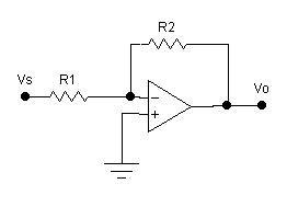
Figure
1 Inverting Operational Amplifier Circuit
2. For Figure 2.
Design and test a non- inverting amplifier with a low-frequency voltage gain of
20 dB.
Ø Use a .TRAN analysis with a 500 mV zero-peak, 1 kHz sinusoidal input
voltage. The input voltage level is not
critical as long as you do not clip your output waveform.
Ø Experimentally verify your design and simulation results in the
time domain.
Ø Measure 20 log|A(jf)| and q(jf) and compare your results with the
SPICE .AC simulation. Extend your measurements to several hundred kHz. Plot your results as you collect the data.
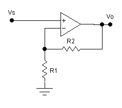
Figure
2 Non-Inverting Operational Amplifier Circuit
3. Refer to circuit diagram given below
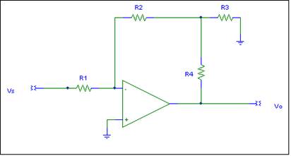
Figure
3 Another Inverting Operational Amplifier Circuit
(a) Derive the voltage gain Vo/Vs transfer function
using summing point constraints. This is
best done as part of your prelab.
(b) Use all 10 kW resistors. Verify
experimentally and using SPICE, the voltage gain at 1 kHz . Use both a time domain and transfer
characteristic representation of your work.
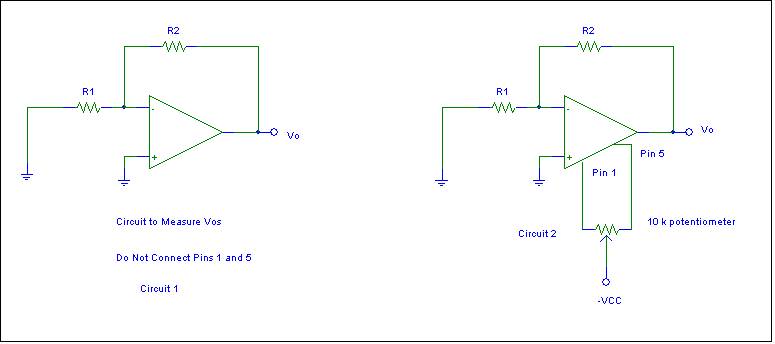
4. Offset Voltage Measurement
(a) Construct Circuit
1 as shown below such that the R2/R1 is nominally 100. Use the DMM to measure the dc voltage at the
output terminal. The dc offset voltage
for the operational amplifier is computed by Vo/100 = Vos
from your measurements. Compare your
results with the data sheet distributed in class. As before, use ±12 volts for the power supplies
and all resistors > 2 kW. Use good lead dress and wiring practices.
(b) Refer to Circuit 2. Connect the potentiometer between Pins 1 and
5 with the center terminal to -12 volts; same as the negative power supply
voltage. Adjust the potentiometer such
that Vos is zero or as close to zero as you can
obtain. How low can you go and how does
this compare to the specifications? Why
is this ability to “zero out” the offset voltage useful in a system design?
To Think About:
Did
the basic operational amplifier model work well in your SPICE simulations. Do the .TRAN and .AC simulations agree with
measurements? This lab seems long but if you come prepared with your circuit
designs all ready to go, it proceeds well.
Observe an unsafe duplex
outlet-no ground pin!

Some
suggestions for wring reports.
And
in due deference to the iPhone5 release last week.