EE 2212
EXPERIMENT 8
5 December 2013
THE EMITTER-COUPLED PAIR
Note 1: A written report is not required. We will jointly review your notebook during
the 12 December laboratory period with the expectation that this experiment
will be included.
Note 2: The CA 3046 is the same electrically as the
LM 3046. Just a
different manufacturer.
PURPOSE
The purpose of this experiment
is to characterize the
properties of a:
Ø The emitter-coupled pair (DC transfer
characteristics)
Ø The
emitter-coupled pair (AC gain measurements).
COMPONENTS
Ø LM3046/CA3046 transistor array. The data sheet is posted on the class WEB
page
Ø Resistors and potentiometers as required
for the current sources.
Ø Three 20 kW resistors for the collector resistors of
which two should be reasonably well
matched
Ø 4.7 kW resistor for the input voltage divider
Ø 47 W resistor for the input voltage divider
GENERAL INFORMATION
Ø In IC biasing networks, it is essential
that transistors be well matched and parameter variations track with
temperature. Figure 1 is a pin out of
the LM3046/CA3046 Transistor Array. Observe that you MUST connect Pin 13, the
IC substrate, to
the most negative point in the circuit or bad things happen to the IC.
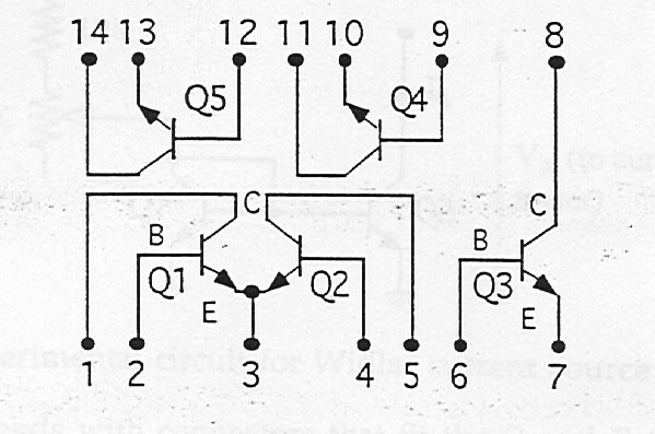
Figure 1 LM3046/CA3046 NPN BJT
ARRAY
.
PRELAB FOR THE EMITTER-COUPLED PAIR
Use Figure 1 and class notes
for guidance to prepare a detailed circuit diagram. Include pinouts
for the LM3046/CA3046 npn
array. From your circuit diagram and circuit specifications, calculate the
expected important Q-point values, and Adm,
Acm, and the CMRR in dB.
DC MEASUREMENTS
Refer to the diagram and data
sheet of the LM 3046/CA3046 BJT array.
Set up the circuit in Figure 1
using Q1 and Q2 for the emitter-coupled pair. Q3 and Q4 form a simple current
source. Ground both the inputs of Q1 and Q2. Measure the all Q-point voltages
and currents using the DMM. Use the oscilloscope to also check for excessive
noise which may translate as a noisy dc voltage measurement. Pay particular
attention to VOD. Since the transistors and resistors are reasonably
well matched, you would expect VOD = 0 or reasonably close. If VOD
is larger than a few tens of mV, check your circuit and/or match the collector
resistors better. Lead dress and length is also important. Be neat! Compare
your Q-point values with the expected and PSPICE simulations. In addition to using the DMM, look for excessive noise using the
scope even though you are measuring the dc voltage matching.
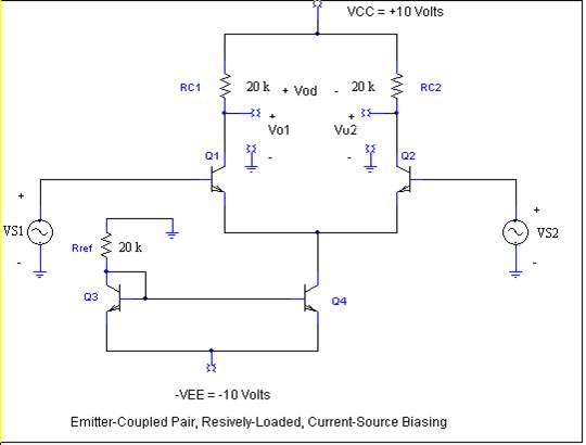
Figure 1
TRANSFER CHARACTERISTICS
The transfer characteristics of
a circuit can be displayed using the X-Y oscilloscope inputs. The amplitude of the
input must be large enough to drive the input through the entire desired range
of operation. You are particularly interested in the VOD versus VID
characteristic. Use a low frequency sinusoid or triangular wave as the input.
From a practical viewpoint, if the input signals are noisy because of low
amplitudes, you may choose to use an input voltage divider to provide
"cleaner" waveforms. Consider implementing the 100:1 voltage divider
input drive circuits, Figure 2, although it doesn’t have to be 100:1. The
signal generators have a 100 mV minimum. By using a 100:1 external divider, you
can achieve a relatively noise free signal at the input to the BJT bases. Keep
track of the divider ratio you finally use to scale your measurement correctly.
Also observe that because the oscilloscope does not have a floating input
(i.e., one side of each oscilloscope input is connected to ground), you will
have to measure either VO1 or VO2 and scale the final
results accordingly by a factor of 2 and also do not forget the sign (180°phase)
differences for each of the outputs.
Show that the slope of the
transfer characteristic will be equal to |Adm/2|.
Compare your results to a SPICE simulation.
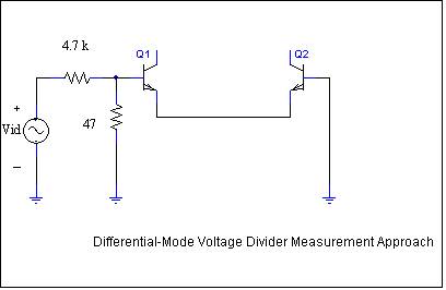
Figure 2
DIFFERENTIAL-MODE OPERATION
Set up your input signals, use 1 kHz, so that the output is reasonably linear.
You will need some level of voltage division as shown in the figure. The figure
illustrates a 100:1 divider but the actual divider value is not critical. Use
the oscilloscope and DMM to measure the differential-mode voltage gain. Compare
your results to your calculations and a SPICE simulation. Include the effect of
a non-infinite Early voltage to improve your analysis
and simulation accuracy.
COMMON-MODE OPERATION
Set up your input signals,
again use 1 kHz., so that the output is reasonably
linear. You will not need an input voltage divider because the Acm is low, Figure 3, because the common-mode voltage gain
is sufficiently low that you will have to increase the input level significantly
above what you used in the differential-mode measurement. That is do not use the 100:1 input divider. Prepare a circuit
diagram illustrating how you are measuring the common-mode voltage gain.. Measure the common-mode voltage gain and compute the
measured CMRR and convert to dB. Compare your results to your calculations and
SPICE simulations.
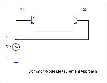
Figure 3
If you decide to pursue
a BSEE degree, you should at least understand the basics of computer engineering. Above and beyond CS1, the following provides
an important understanding of computer technology hardware.
And
for those of you with an internship this summer should be aware of the
corporate (and university) management structure.