EE 2212
EXPERIMENT 7
20 November 2014
BJT CURRENT SOURCES –Revised
Note 1: Report is due Thursday, 4 December.
Note 2: We will use the laboratory time slot on
Thursday, 11 December, for individual notebook reviews.
Note 2: The CA 3046 is the same electrically as the
LM 3046. Just a different manufacturer.
PURPOSE
The purpose of this experiment
is to characterize the
properties of a:
Ø Basic/Simple Current Source
Ø Widlar Current Source
COMPONENTS
Ø LM3046/CA3046 transistor array. The data sheet is posted on the class WEB
page
Ø Resistors and potentiometers as required
for the current sources.
PRELAB
Compute the values of the
resistors you will need to evaluate the simple and Widlar
current sources at the indicated current levels.
GENERAL INFORMATION
Ø In IC biasing networks, it is essential
that transistors be well matched and parameter variations track with
temperature. Figure 1 is a pin out of
the LM3046/CA3046 Transistor Array. Observe that you MUST connect Pin 13, the
IC substrate, to
the most negative point in the circuit or bad things happen to the IC.
Ø The only reason there is a fixed 10 kW resistor in the circuit is to protect the
BJT against inadvertent application of a high voltage across the Base-Emitter
junction as you adjust the potentiometer.
You do not want to apply 15 volts to the base of Q1 because the chip
becomes toast (literally and figuratively)!!!
Effectively, the series combination of the 10 kW resistor and the potentiometer is the RREF.
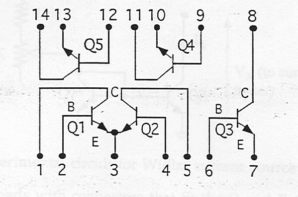
Figure 1 LM3046/CA3046 NPN BJT
ARRAY
SIMPLE CURRENT SOURCE
Figure 2 is a schematic diagram
of a simple current source.
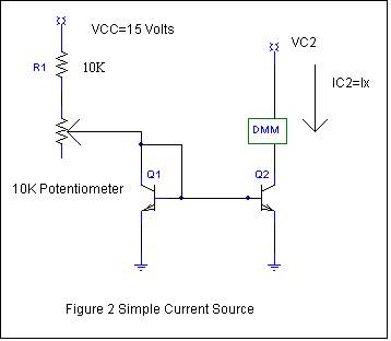
Connect the collector of Q2,
(VC2) to a 5-volt DC supply. Place a DMM in series with the Q2 collector lead
to measure current. If the internal fuse
in your DMM is open, replace the DMM with a 1kΩ resistor and measure the voltage
across the resistor and use your results to compute the current. Set IC2=IX to 1 mA by adjusting
the 10 kΩ potentiometer. Compare this value to the reference
current. Measure all key currents and
voltages. Construct the I-V output characteristic by changing VC2 from 0 to 5
volts. Obtain the output resistance
from the slope. Compare to a SPICE simulation.
WIDLAR CURRENT SOURCE
Figure 3 is a schematic diagram
of a Widlar current source.
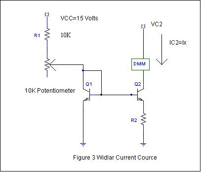
For a reference current of 1
mA, compute the value of R2 required to obtain Ix = 100 mA ±10%. Note that VCC = 15 volts. Now
connect the collector of Q2 (VC2) to a 5-volt DC supply. Place a DMM in series
with the Q2 collector lead to measure current.
If the internal fuse in your DMM is open, replace the DMM with a 1kΩ resistor and
measure the voltage across the resistor and use your results to compute the
current. You may have to change the
value of R2 from the computed value to come within 100 mA ±10% .
Measure all key currents and voltages. Sketch the I-V output characteristic from VC2
from 0 to 5 volts.. Compare these results with the simple current source
results. You will have to measure
carefully because the slope will be close to flat as you would expect. Compare to a SPICE simulation.
Not quite a TESLA but getting
there

For Next Week

After All, This A Lab