EE
2212
POWER
AMPLIFIER RELATED PROBLEMS
FINAL
EXAM PREPARATION
S.
G. Burns
I
strongly recommend that you review text pages 1006 through 1012 as well as our
class discussions related to power amplifiers prior to the Final Exam. In addition to some text problems, I have provided an
amalgamation of sample problems from old
quizzes and final exams that include
power amplifier topics. I do like to use
real circuits as the basis for problems.
The
problems will not be collected but I strongly suggest you bring copies of your
solutions to the Final Exam
1.
Text 15.102. Also sketch and label the back-to-back load
lines.
2.
From an old quiz.
Assume a Class B audio amplifier
operating between ±48
volts and driving a 4 W speaker. Neglect the
effect of crossover distortion.
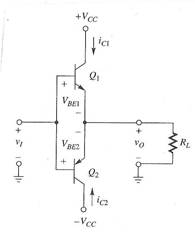
(a)Provide
required maximum ratings as indicated for the transistors using a well-labeled
sketch of the back-to-back load lines to illustrate your answers.
IC(max) = ____________ VCE(max) = ___________ PC(max) = __________
(b)
Design a protection circuit to limit the
transistor to the IC(max) you computed in part (a) should the amplifier output be
short-circuited. Incorporate this protection
circuit in your basic Class B circuit diagram.
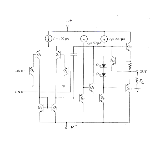
3. Amplifier
Analysis
A partial circuit diagram
for a Fujitsu MB 47358 operational amplifier is given below. Assume V+ = 15 volts and V-
= -15 volts. For the npn
transistors, assume b = 150, VBE(on) =
0.7 Volts, and VAN = 100 Volts.
For the pnp transistors, assume b = 100, VBE(on) = 0.55 Volts, and VAP
= 50 Volts.
(a) Briefly describe the circuit function/operation of :
Q10 and Q11
Q13 and Q14
(Diode connected transistors)
Q7 Circuit
topology
Q5 and Q6
(b) Assume a
sinusoidal input voltage that results in an output voltage vo(t) = 12 sin (wt)
volts. RL = 1 kW.
Compute
values for :
1. Peak
and average power to the load resistor.
2. Resultant
collector efficiency.
3. Power
required from the power supplies for the output stage.
4. A
design value for RSC to limit the short circuited load current to 30
mA .
(c) Estimate the following :
1. Collector
currents in Q5 and Q6
2.
Collector currents in Q1 and Q2
3.
Voltage at the base of Q5 and Q6
4. Voltage
at the emitter of Q7
4. Power Amplifiers
I had a problem
similar to this on a past final exam.
Who know? Something like this
could be on the Final in a couple of weeks!
Look at Review Text 15.107.
Follow the same approach we used for a sinusoidal signal and look at Text
15.108. Think Class D to provide a
one-line answer. Note the similarity.
(a) In class, for a Class B (AB) amplifier, we
derived the collector
efficiency for a sinusoidal signal with a maximum value of 78.5%.
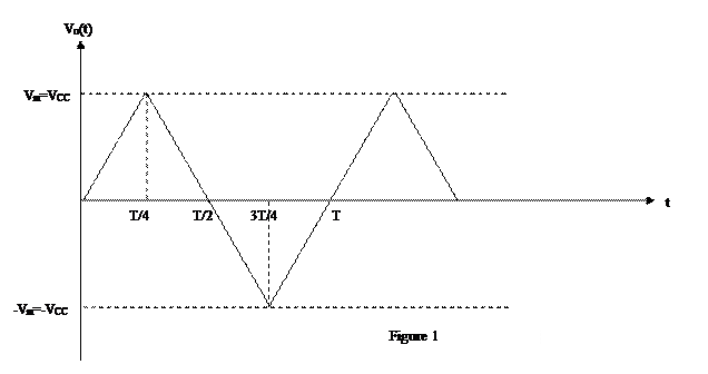
Now consider a periodic triangular signal shown in Figure 1.
Derive the maximum collector efficiency, hC, for this
waveform. I suggest using symmetry to
minimize the algebraic effort.
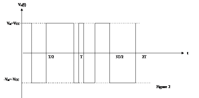
(b) By inspection, (no calculations are necessary) provide a value for the approximate
collector efficiency, hC, for the Figure 2 waveform.
Explain your answer.