EE
2212
PROBLEM
SET 7
S.
G. Burns
Due: Wednesday, 26 October 2016
1. Similar
to the NMOS version from Problem Set 6. Text
4.49 PMOS. In
addition to answering the questions, refer to Text Figure P4.49 associated with
Text Problem 4.49 and using the SPICE
example I demonstrated in class, generate a SPICE PMOS model by modifying the
default PMOS transistor that will match
the curves in P4.49 figure. We did not
generate the PMOS curves in Experiment 4, but the approach is similar. Observe that Figure P4.49 is given as a first
quadrant plot but the axes are labeled appropriately for the third
quadrant. Again, if you look at the
curves, it is a good assumption that λ = 0. Your problem submission must include the
listing of your modified MOS parameters and the resultant ID-VDS
curves as a function of VGS. This will be a third-quadrant plot.
2. Refer
to Figure 6.17(d) on text page 306 and the more detailed version shown in
Figure 6.22(a) on page 315. Using the
data supplied in Figure 6.22(a), use a SPICE simulation to obtain a reasonable
match to the transfer characteristic shown in Figure 6.22(b). Submit your circuit diagram, FET model and
attribute data, and the transfer characteristic.
3. Extracted
and modified from an from an old quiz.
(a)
The
CMOS inverter consists of
(NMOS ENHANCEMENT MODE, NMOS DEPLETION 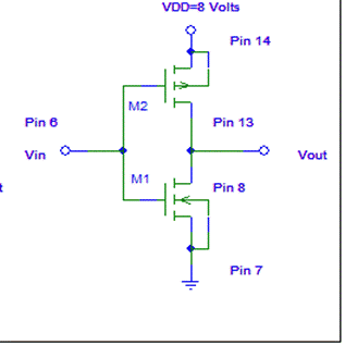 MODE, PMOS ENHANCEMENT MODE, PMOS DEPLETION MODE)
transistors. Circle your choices.
MODE, PMOS ENHANCEMENT MODE, PMOS DEPLETION MODE)
transistors. Circle your choices.
(b)
Sketch
and label the transfer characteristic.
Label the regions where M1 is ON and OFF, M2 is ON and OFF, the region where the circuit can
be used as an amplifier, the Q-Point yielding the highest power dissipation.
(c) The CMOS inverter static power dissipation
is (COMPUTED FROM THE SLOPE OF THE TRANSFER CHARACTERISTIC,ESSENTIALLY ZERO,
COMPUTED FROM P=(VI)/![]() ) . Circle your choice.
) . Circle your choice.
(d)
The
input resistance of a CMOS INVERTER is (ESSENTIALLY ZERO, COMPUTED FROM R=V/I,
Essentially ∞). Circle your
choice.
The following problem refer to switched capacitor design which
I anticipate discussing on Monday, 24 October.
4. Design a switched
capacitor circuit that could be used in place of a 10 kW resistor where the maximum frequency of any
signal does not exceed the typical audio
bandwidth of your smart phone Your
design should include:
· Well-labeled circuit diagram
· Key component values and an appropriate clock
frequency
· Waveforms as appropriate
Pot-Pourri From My Vast Files Of Stuff
For your
career and internship “guidance”
As
you can observe from my Google calendar I post on the WEB and on my door, I go
to lots of meetings, many with minimal utility.
You will also have many meeting
“opportunities” during your engineering
career. The following is so true: