EE 2212
Spring 2013
7 and 14 February 2013
Experiment 2: Operational Amplifier
Circuits
Report Due: 21 February
Note 1: This will be a two-week experiment (7 and 14 February). I will suggest a natural break point but you are
encouraged to proceed at your own pace.
It will be graded on a 40-point scale with double the values on the
20-point rubric.
Note 2: The afternoon lab section on 7 February will
end at about 2:30 because I will have to leave.
Sukriti will be at the UM Career Fair in the
Cities and will be unable to be present after I leave at 2;30.
Note 3: I will provide an overview of the op amp
SPICE models at the beginning of the lab.
PURPOSE
Week One
Ø
To implement the
designs of inverting and non-inverting amplifiers using an operational
amplifier.
Ø
To modify the
SPICE frequency-independent model to simulate the measured frequency response
of the inverting operational amplifier
configuration.
Ø
To compare the
SPICE model discussed in class with the SPICE Schematic capture library model
which will include frequency effects.
You
can continue into Week 2 tasks as appropriate.
Week
Two
To
implement the designs of:
Ø An active analog Low-Pass Filter (LPF)
Ø An active analog High-Pass Filter (HPF)
Ø A Wien Bridge Oscillator
Ø A Phase Shift Oscillator
PRELAB
FOR WEEK ONE
Design the circuits to
meet the indicated specifications. You should come to the lab with a list of
the components you will need to meet the specifications. You might refer to your
ECE 2006 notes and labs since many of you have worked with op amps in that
course. Write and run SPICE time and
frequency domain programs for both circuits.
Use the LIB 741 model if you have it in your
version of SPICE and use the linear model presented in class or the generic “op
amp” in the LIB file. Print the
waveforms of the inputs and outputs on the same set of axes. You will need the
following information from your SPICE program in order to complete this lab:
Ø
3 dB BW, key
amplitudes, and times
Ø
.AC analysis of
frequency and phase
Ø
.TRAN analysis
Ø
Derivation of the
voltage gain for Circuit 3.
Your designs should
not incorporate series and parallel resistors to meet the voltage gain
specifications. It is more desirable to
come close with standard value components and use the exact numbers in your
circuit and simulation.
PROCEDURE
Refer to
the mA741
data sheet on the class WEB page uA741.pdf,
also distributed in class. Observe, you are using the 8-pin DIP (Dual-Inline Package) Second package style from the top. Also note that the mA741 has certain requirements with respect to allowed
resistance values. All resistors in your design must be
greater than or equal to 2 kW. You do not need to include
the 10 kW offset
voltage potentiometer initially in your circuits for the first three circuits.
Use ±
12 volts for the power supplies. Verify
that the polarities are correct or ![MM900336554[1]](Experiment2OperationalAmplifierCircuits_files/image002.gif) you will create a classic embarrassing odor.
you will create a classic embarrassing odor.
Your
designs should be supported analytically and by SPICE simulation results. You should record all key oscilloscope
waveforms on your flash drive as support
for your laboratory report.
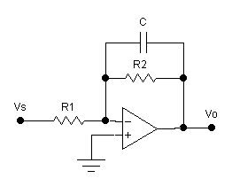
1. For Figure 1. Design and test an
inverting amplifier with a low-frequency voltage gain of 20 dB.
Ø
Use a
transient analysis with a 500 mV
zero-peak, 1 kHz sinusoidal input voltage.
The input voltage level is not critical as long as you do not observe
clipping on your output waveform.
Ø
Experimentally
verify your design and simulation results in the time domain.
Ø
Experimentally
determine the input signal level when
“clipping” of the output waveforms occur.*
Does the simulation using a linear circuit operational amplifier show
this clipping? Explain. Compare to the simulation using the library
model in SPICE.
Ø
Measure and plot
20 log|A(jf)|, voltage gain as a function of frequency, and q(jf),
which is the phase shift as a function of frequency, through the amplifier
circuit, and compare your results with the SPICE AC simulation. Extend your measurements to a few hundred kHz if you can. Plot the results as
you take your measurements.
Ø
In your SPICE AC
simulation using the linear model or the generic op amp model in the .LIB file,
place a capacitor between the inverting node and the voltage-controlled
generator node of such a value that the simulation matches the experimental
measurement of the 20 log|A(jf)| plot reasonably well. How does your model compare with the SPICE
library 741 model? As we have discussed
in class, the mA741 model simulation we did in class was frequency independent
because there was no capacitor or inductor in the model or the rest of the
circuit.
* You should do this in the time domain and observe the transfer characteristic. In order to see the transfer characteristic
on the digital oscilloscope, you will need to change the display to “XY”
mode. Push the “Display” key and select
“XY Display” from the menu. Switch to
“Triggered XY” mode. You may use the
scale controls to adjust the axes accordingly.
Also verify your voltage gain and phase shift measurements using the
transfer characteristic. Do not overdo
the input voltage to observe clipping because if your input becomes too large,
you will damage the mA741.
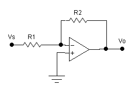
Figure
1 Inverting Operational Amplifier Circuit
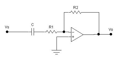
2. For Figure 2. Design and test a non-
inverting amplifier with a low-frequency voltage gain of 20 dB.
Ø Use a transient analysis with a 500 mV zero-peak, 1 kHz sinusoidal input
voltage. The input voltage level is not
critical as long as you do not clip your output waveform.
Ø Experimentally verify your design and simulation results in the
time domain.
Ø Measure 20 log|A(jf)| and q(jf)
and compare your results with the SPICE AC simulation. Extend your measurements
to several hundred kHz. Plot your
results as you collect the data.
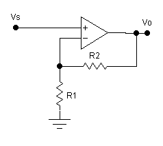
Figure
2 Non-Inverting Operational Amplifier Circuit
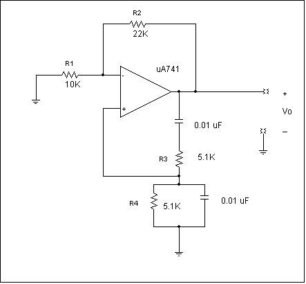
3. Refer to circuit diagram given below
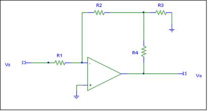
Figure
3 Another Inverting Operational Amplifier Circuit
(a) Derive the voltage gain Vo/Vs transfer function using summing point
constraints. This is best done as part
of your prelab.
(b) Use all 10 kW resistors. Verify experimentally
and using SPICE, the voltage gain at 1 kHz .
Use both a time domain and transfer characteristic representation of
your work.
To Think About:
Did
the basic operational amplifier model work well in your SPICE simulations. Do
the transient and AC simulations agree
with measurements?
PRELAB FOR WEEK TWO
Design the Low Pass and High
Pass Filters to meet the indicated specifications. You should come to the lab
with a list of the components you will need to meet the specifications. For the
Low-Pass Filter, the corner frequency is computed from  and the low frequency
voltage gain is given by
and the low frequency
voltage gain is given by ![]() and for the High-Pass
Filter,
and for the High-Pass
Filter,  and the high frequency
voltage gain is given by
and the high frequency
voltage gain is given by ![]() . The derivation of
the corner frequencies follows that of the passive RC filter circuits from
Experiment 1, Problem Sets and the class notes.
Include the derivations in your notebook.
. The derivation of
the corner frequencies follows that of the passive RC filter circuits from
Experiment 1, Problem Sets and the class notes.
Include the derivations in your notebook.
PROCEDURE
Refer to the mA741 data sheet. Observe, again that you are
using the 8-pin DIP. You do not need to include the 10 kW offset voltage potentiometer. All resistors
must be at least 2 kW. Use ± 12 volts for the power supplies. Your Low Pass, High Pass
and Band Pass filter designs should be supported analytically and by SPICE
simulations. Use the library model for the mA741.
Always look at your output waveforms experimentally to insure you are
not clipping.
Explain why you will observe
clipping when you use the mA741 while performing a transient
simulation and you will not observe clipping when you use the generic op
amp model which consists of only a voltage-controlled generator.
1.
Design
and test an low-pass filter with a low-frequency voltage gain of 20 dB and a 3
dB corner frequency in the range of 3
to 5 kHz. Do not use series and parallel capacitor
combinations or series and parallel resistor combinations . Use standard values that yield a corner
frequency and voltage gain reasonably
close to the specifications. The theory
of operation was discussed during the 4 February class.
Ø Experimentally verify your design and
simulation results.
Ø For verifying low-pass filter operation,
measure 20 log|A(jf)| and q(jf) and compare your results with the SPICE AC simulation over a
similar range.
2. Design and
test a high-pass filter with a high-frequency voltage gain of 20 dB and a 3 dB
corner frequency in the range of 100 Hz to 500 Hz. Do not use series and parallel capacitor
combinations or series and parallel resistor combinations. Use standard values that yield a corner
frequency and voltage gain reasonably
close to the specifications
Ø Experimentally verify your design and
simulation results.
Ø For verifying high-pass filter operation,
measure 20 log|A(jf)| and q(jf) and compare your results with the SPICE AC simulation over a
similar range.
3. Construct the
following circuit which is similar to what is shown in Figure 12.45 on page 755
of the text. At first glance, the
circuits look different but they are the same.
You are generating a signal source, that is you are demonstrating
the operation of an oscillator. Observe
that there is no external signal generator!
Monitor Vo(t) using your oscilloscope. Observe there is no input signal. This is called a Wien Bridge Oscillator. Explain why this is a useful circuit. (Note depending upon the resistor tolerances
and circuit losses, you may have to increase your value of R2 somewhat; perhaps
as high as 33 kΩ). Lead dress has
an impact on the circuit performance.
Compare the observed frequency of operation to the equation, ![]() and the voltage gain
required setting established by
and the voltage gain
required setting established by![]()
The
SPICE simulation approach is interesting and I will demonstrate this when we
get to lab. In a real circuit, an
oscillator starts through random noise which provides an initial signal with
the correct phase shift to obtain positive feedback . I like to compare an oscillator starting
with the howling noise you have all heard in a public address system when the
microphone is in the speaker sight range.
To show this in a SPICE simulation, add an initial condition of several
volts to each of the capacitors and then use a .TRAN analysis that extends for several
periods of the expected frequency output.
The signal growth is kind of cool to watch during the simulation.
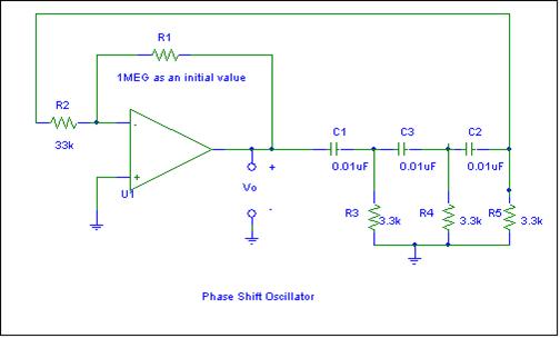
4. Construct the
following circuit similar (but not exactly like) to what is shown in Figures 12.47 and 12.48
on page 756 of the text. Monitor Vo(t) using your oscilloscope. Observe there is no input signal. This is called a Phase Shift Oscillator. Explain why this is a useful circuit. (Note depending upon the resistor tolerances,
you may have to increase your value of R1). Compare the observed frequency of
operation to the equation, ![]() and
the voltage gain required setting established by
and
the voltage gain required setting established by ![]() As with the Wien Bridge oscillator SPICE
simulation, add an initial condition of
several volts to each of the capacitors and then use a .TRAN analysis that extends
for several periods of the expected frequency output. Again, it is interesting and fun to watch the
signal growth as a function of time.
As with the Wien Bridge oscillator SPICE
simulation, add an initial condition of
several volts to each of the capacitors and then use a .TRAN analysis that extends
for several periods of the expected frequency output. Again, it is interesting and fun to watch the
signal growth as a function of time.
Observe an unsafe duplex
outlet-no ground pin!
Some suggestions for
writing laboratory reports.

For
those of you who are “trekies” i.e. fans
of Star Trek