EE 2212
POWER AMPLIFIER RELATED PRACTICE
PROBLEMS
2 May 2013
I strongly recommend that
you review text pages 1006 through 1012 prior to the Final Exam. Also I have
provided an amalgamation of three sample problems from old quizzes and final
exams that include power amplifier topics. I do like to use real circuits as the
basis for exam problems.
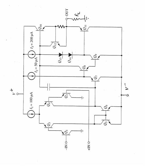
Review Problem 1 (Amplifier Analysis)
A partial circuit
diagram for a Fujitsu MB 47358 operational amplifier is given on the next page.
Assume V+ = 15 volts and V- = -15 volts. For the npn transistors, assume b = 150, VBE(on) = 0.7 Volts, and VAN
= 100 Volts. For the pnp transistors, assume b = 100, VBE(on) = 0.55 Volts, and VAP
= 50 Volts.
(a) Briefly describe the circuit
function/operation of :
Q10 and Q11
Q13 and Q14
Q7
Q5 and Q6
(b) Assume a sinusoidal
input voltage that results in an output voltage vo(t) = 12 sin (wt) volts. Observe that RL
= 1 kW.
Compute
values for :
1.
Peak
and average power to the load resistor.
2.
Resultant
collector efficiency.
3.
Power
required from the power supplies for the output stage.
4.
A
design value for RSC to limit the short circuited load current to 30
mA .
(c ) Estimate the following :
1.
Collector
currents in Q5 and Q6
2.
Collector
currents in Q1 and Q2
3.
Voltage
at the base of Q5 and Q6
4.
Voltage
at the emitter of Q7
Review Problem 2 (Power
Amplifiers)
(a) In class, for a
Class B (AB) amplifier, we derived the collector efficiency for a sinusoidal signal with a maximum
value of 78.5%. Now consider a periodic triangular signal shown in Figure 1. Derive the
maximum collector efficiency, hC, for this waveform. I
suggest using symmetry to minimize the effort.
(b) By inspection, (no calculations are
necessary) provide a value for the approximate collector efficiency, hC, for the Figure 2 waveform. Explain your answer.


Practice Problem
Class AB Power Amplifier Analysis.
For this Class AB amplifier, assume VCC = 40 volts and
the minimum allowable value of RL = 4 .
Sketch and Label back-to-back
load lines. From your load lines,
provide values for BJT specifications of IC(max),
VCE(max) , and PC(max) required for each transistor so they are not damaged.
Assume a sinusoidal output given by ![]() . Compute the collector
efficiency for:
. Compute the collector
efficiency for:
Vm =
30 volts
Vm
= 40 volts.
Assume a sinusoidal output given by ![]() where Vm = 40 volts. Compute a minimum value for the power output
capability required of the dc power supply.
where Vm = 40 volts. Compute a minimum value for the power output
capability required of the dc power supply.
Suppose, RL is short-circuited
(oops) Design
an over-current protection circuit to protect both Q1 and Q2. By design, you are to add circuits to the
circuit diagram with appropriate sampling resistor values such that the value you obtained in Part (a)
for IC(max) is not exceeded for both Q1 and Q2.
By inspection, (no calculations are necessary) provide a value for the approximate
collector efficiency, hC, for the following waveform. The waveform shown in Part (b) would indicate
that the circuit is now operating in (CLASS A, CLASS B, CLASS C, CLASS D). Circle your choice. Briefly Explain your answer in the context of the back-to-back load
lines.
