ECE 2212
PROBLEM SET 10
S. G. Burns
Due: Friday,
19 April 2013
Note: I will be at the SME
Conference Tuesday All Day and Wednesday morning (16 and 17 April) of next week.
To provide additional opportunities to ask questions and for office hour
consultations, I am scheduling Quiz 10 for Friday, 19 April, rather than
Wednesday, 17 April. By the way,
students are invited to attend. http://www.d.umn.edu/ce/learningopportunities/conferences/sme/
1. Text
5.83. Part (a) only and Text 5.84
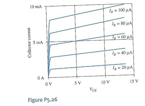
2. Refer to Text
Figure P5.26 given below. Modify the
default BJT SPICE model to generate a set of curves that are a reasonable match
to the characteristics shown in Figure P5.26.
Save this model because you will need it in Problems 3 and 4. Submit the BJT non-default model parameters and
a copy of the characteristic curves that you obtained. Key parameters to change will be β and
VAF.
3. Text 5.94 and
compare your Q-Point analytical results with a SPICE simulation using the BJT
SPICE model results from Problem 2.
Depending upon your version of SPICE, the Q-Point could also be called
the Operating Point, OP,
or the Bias Point. You
select this from the Setup Menu.
4. Text 5.97. Observe
that you will have to derive an equation for the base current by summing
current at the collector node. Again, compare your Q-Point analytical results
with a SPICE simulation using the BJT SPICE model results from Problem 2.
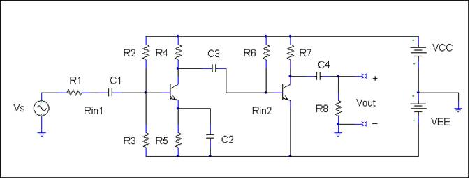
5. This
is a circuit of a two-stage npn-npn cascade amplifier
operating between two power supplies, VCC and a -VEE.
Assume that for BJTs Q1 and Q2, IC1 = 1 mA
and IC2 = 2 mA, b1 = 100 and b2 = 150, and both Early voltages
are 75 volts.
(a) Draw and label a small-signal, frequency-independent, model. By
frequency-independent I mean that the you should
assume capacitive reactances are very small at the
frequency of interest.
(b) Using your small-signal model, derive an algebraic equation for
the voltage gain defined by Av
= Vout/Vs.
(c)
Compute
numerical values for gm, ro,
and rp
for both the npn BJTs.
(d)
Using your small-signal model, derive an
algebraic expression for the input resistance Rin1 and Rin2.
Q2 Q1
![]()
![]()
I have a collection of these!