EE 2212
PROBLEM SET 5
S. G. Burns
Due:
26 February 2013
1.
Text 3.72 Part (a)
assumes you assume the diode switches from OFF to ON when the diode voltage is
zero volts. Part (b) of problem assumes you
use the diode model that just includes a 0.7 volt battery when the diode
switches from OFF to ON. The best
approach is to draw out each circuit and then look for any potential
contradictions with the diode model and circuit when you assume a diode is either
ON or OFF. Sketching a piece-wise linear
I-V characteristic is one approach to piece-wise linear problems. Prepare a table to summarize your results.
2.
Based
on an old quiz problem. You are to design a battery charger for safe operation in a damp
garage environment to
use for charging your 12 VDC car
battery.
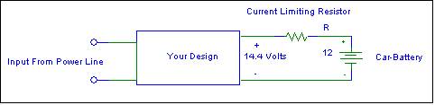
Design, that is provide a detailed and
well-labeled circuit diagram, a dc power
supply to accomplish this objective by satisfying the following design
specifications:
(a)
Input
is a 110rms VAC. (VP=110x ![]() ) at 60 Hz from a three wire service that
meets the National Electrical Code.
) at 60 Hz from a three wire service that
meets the National Electrical Code.
(b)
Output
is a nominal 14.4 VDC
(c)
Specify
a resistor, R, to
limit the maximum battery charging current to 10 amperes.
(d)
Use
a half-wave rectifier.
(e)
There
is no ripple voltage design specification.
Explain why this is unnecessary in this application.
(f)
Use
a transformer .
(g)
The
battery charger case is metal.
(h)
Assume
a diode with VF = 0.7 V
(i)
Use
a correctly located fuse in the primary circuit to protect the power supply
from a short-circuit at the battery terminals either
from total battery failure or accidentally short  circuiting the charging cable to ground. (For
example, dropping a wrench across the battery terminals-oops!).
circuiting the charging cable to ground. (For
example, dropping a wrench across the battery terminals-oops!).
(j)
A
voltage regulator is not required
Your Design must include:
Well-labeled circuit diagram including the identification of the incoming “hot”, “neutral”, and “ground wires (U.S.
standards) including the National Electric Code color coding of these wires and
also show the correct color-coded wiring for a standard grounded duplex
receptacle and plug.

i.
Key
design equations and supporting calculations
ii.
Component
specifications including:
iii.
Transformer-turns
ratio
iv.
Diode-current
and power ratings
v.
Your
assessment and short discussion as to whether the laboratory 1N4001 diodes
would work or not.
vi.
Value
for R
vii.
Current
rating of a fuse to protect the power supply against a short circuit condition
at the battery terminal.
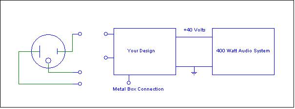
3.
Similar to an old quiz
problem. Your design team is to design a +40
volt dc power supply for your home sound
system. Your sound system requires a 400 watt
capability. The power supply is
energized from a three-wire 110 Vrms 60 Hz power line
that meets the National Electric Code (NEC).
The system
block diagram and design specifications are given below.