ECE 2212
PROBLEM SET 8
S. G. Burns
Due: 3 April 2012
Note 1: Recall that you obtained a SPICE model for
Figure P4.18 on Page 205 of the text when you provided a solution to Problem Set 7, Problem
2 Text 4.18 NMOS . You will be using this model to compare
solutions when you solve Problems 1 and 2.
This requires you need to use the “Bias Point Detail” in the SPICE
Analysis setup.
Note 2: The first three problems are finding the
Q-Point of several types of biasing configurations. Problem 4 is a SPICE simulation patterned
after what we are doing in class.
1. Text 4.89 Compare with the Bias Point Detail
SPICE results.
2. Text 4.92 Compare with the Bias Point Detail
SPICE results.
3. Text 4.111 No SPICE required.
4. Refer to the depletion-mode inverter that
we will discuss in
class on 27 and 29 March. Also refer to Section 6.6 in the text and more
specifically, Figure 6.23 on Page 316. Let VDD= 10 volts. Use a SPICE simulation to generate the vO versus vIN transfer characteristic. Your solution should include:
Ø Schematic capture circuit diagram
Ø SPICE generated iD-vDS characteristics for the depletion-mode
transistor.
Ø SPICE generated iD-vDS characteristics for the
enhancement-mode transistor.
Ø SPICE generated transfer characteristic vout versus vin with all key points labeled and
explained.
Use the
following transistor specifications
Transistor M1 (MS) M2_(ML)_____
k (not KP) 200
mA/V2 200 mA/V2
Vt +2.5
volts -2.5 volts Note sign changes
W, L W=L W=L
l 0 0
5. Adapted From Several Old Quizzes
Switched Capacitor Low Pass Filter
Design We will
discuss this topic on Friday 29 March or Monday, 1 April.
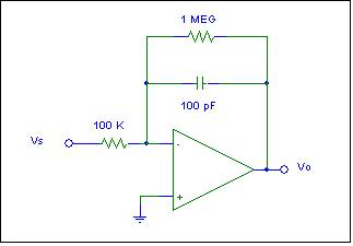
(a)
Sketch and label the voltage
gain of this circuit, 20 log |A(jf)|.
Refer to the first couple of weeks of the semester when we studied active
analog low-pass filters.
(b)
Redesign this circuit as a
switched capacitor filter. Your design should include:
·
Well-labeled circuit diagram.
·
No resistors-That is replace the two resistors with
switched capacitors. Your design should include appropriate W/L ratios.
·
An appropriate clock frequency for operation at input
signal frequencies to 10 kHz.
·
Key waveforms illustrating the operation.
FOR DC, Of COURSE
AS AN ELECTRICAL ENGINEERING STUDENT, MAYBE YOU WERE ASKED TO
DO THIS
WHEN YOU WENT HOME OVER SPRING BREAK.

and Students and Faculty
![]()