EE
2212
PROBLEM
SET 9
S.
G. Burns
Due:
Wednesday, 10 April 2013
Note: I am looking for circuit diagrams and
specifications for audio power amplifiers that you may have for some of your
“stuff”. Information such as circuit
diagrams, specifications for your sound systems, guitar amps, car
stereos, powered sub-woofers, associated power supplies, speaker systems,
etc. The meaner and badder
the better! I would like to borrow the
material to supplement our class discussions on power amplifiers in a few weeks.
We
have been using the CMOS CD 4007 IC in lab the last three weeks. There is a large family of logic and Boolean
functions available in
the 4XXX family. These two additional problems on CMOS will assist you in
understanding the concepts you demonstrated during
the 4 April laboratory.
- The following is a circuit diagram from the CMOS 4XXX
series of ICs. Assume VDD =
5 volts and is a LOGIC ONE and VSS = 0 volts is
a LOGIC ZERO
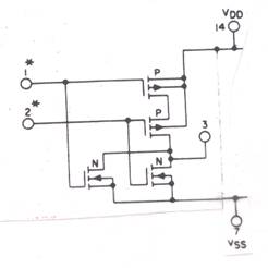
Fill in the following table and indicate which
Boolean function is being implemented.
|
Pin 1 |
Pin 2 |
Pin 3 |
|
0 |
0 |
|
|
0 |
1 |
|
|
1 |
0 |
|
|
1 |
1 |
|
Boolean Function
being implemented:___________________________
- The
following is a circuit diagram from the CMOS 4XXX series of ICs. Assume VDD = 5 volts and is a
LOGIC ONE and VSS = 0 volts is a LOGIC ZERO. When you study this circuit, you will
observe that the circuit in Problem 1 is embedded as a sub-circuit in this
problem. You may find it
convenient to mark up the diagram with intermediate logic levels as you
work your way through the circuits.
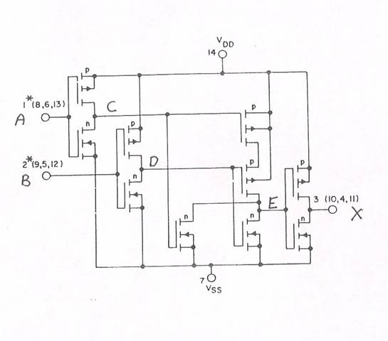
Fill in the following table and indicate which Boolean function is
being implemented.