ECE 2212
PROBLEM SET 10
S. G. Burns
Due: Wednesday, 23 April 2014
Study selected portions
of text Sections 16.2 through 16.5 related to basic and Widlar
BJT Current Mirrors as
well as the class discussions we started on Monday, 14 April. Class discussions on Friday will provide
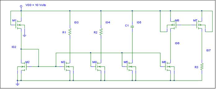
background for the MOS current sources to be studied in Problem 3 and 4.
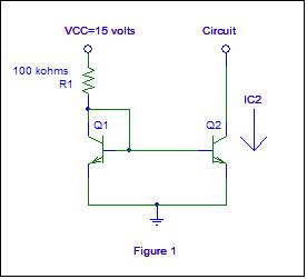
1. Simple and Widlar Current Sink and
Source Calculations
(a)
Compute a value
for IC2 which is the current you would sink from a circuit requiring
that current bias level.
(b)
Design a pnp circuit based upon the npn
circuit shown in Figure 1 that would operate as a current source, rather than a
current sink, for the current computed in Part (a). Your design must include a
well-labeled circuit diagram.
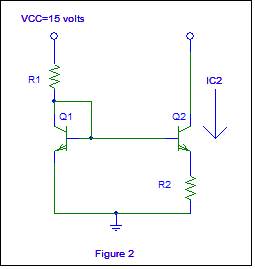
(c)
Design a Widlar current source to sink the current computed in Part
(a). Refer to Figure 2. You have a fair amount of flexibility in R1 and R2.
Follow guidelines presented in Wednesday’s, 16 April, class discussions.
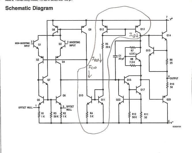
2. The following is a circuit diagram of a National Semiconductor LM
741 operational amplifier. Recall from the beginning of the semester that you
will be able to analyze key sub-circuits of operational amplifiers and related
circuits by the end of the course. I
have circled key elements of the current source system you are analyze. Assume
all |VBE(on)| = 0.7 volts. V+
= 12 volts and V- = -12 volts. All npn transistors have equal junction areas and all pnp transistors have equal junction areas. The Fairchild μA 741 diagram on text page 1097, Figure 16.46, is
another variation. I prefer to use the National Semiconductor LM 741 circuit
diagram and Signetics μA
741 circuit diagram because they are a bit easier to read. There are
differences in some component values because they originate from different
manufacturers. I suggest studying the
example in Section 16.9.2.
Compute values for IREF, IC10, and I13.