ECE
2212
PROBLEM
SET 7
S.
G. Burns
Due: Wednesday, 2 April 2014
1. Refer to the sketch of
an n-channel enhancement-mode MOSFET fabricated in silicon. Assume room
temperature operation. Also
assume l = 0. Units are important
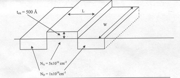
![]()
(a)
Compute
a value for Cox .
(b)
Compute
a value for the threshold voltage, Vt
using the threshold voltage graph posted on the WEB page.
(c)
Assume
W/L = 10 and make reasonable assumptions and/or use values from Table 4.6 for
any other physical parameters you may need. Compute values for “k” and “KP” and
then use your results from this part and Parts (a) and (b) to generate a Sichmann-Hodges Level 1 model equation.
(d)
Using
your calculated results from Part (c), sketch and numerically label the iD versus vDS
as a function of VGS curves. Label the Saturation, Cutoff, and Ohmic (Triode) regions.
2. Text 4.18 NMOS . In addition, refer to Text Figure P4.18
associated with Text Problem 4.18.
Using the SPICE example I demonstrated in class, generate a SPICE
program by modifying the default NMOS transistor that will match the curves in P4.18
figure. If you look at the curves, it is
a good assumption that λ = 0. Also note that extracting MOS parameters
from the graphical output has been used on old quiz problems. Recall, I asked
similar model analysis for diodes.
3.
Text 4.49 PMOS In addition, refer to Text Figure
P4.49 associated with Text Problem 4.18.
Using the SPICE example I demonstrated in class, generate a SPICE program
by modifying the default PMOS transistor that will match the curves in P4.49
figure. Again, if you look at the
curves, it is a good assumption that λ = 0. Also note that extracting MOS
parameters from the graphical output has been used on old Quiz problems.
Recall, I asked similar model analysis for diodes.
Problems 4, 5, and 6 provide practice in working with
small-signal models. Use the basic voltage-controlled current generator FET
small-signal model with λ (Lambda) =0.
In addition to answering the text questions, you are to draw and label
the resultant small-signal model circuit diagram for Problems 4, 5 , and 6. These
three problems also will familiarize you with the text FET symbol notation.
4.
Text 13.5 After you have obtained the
small-signal model, derive an equation for the voltage gain defined by av = vo/vi. Observe that no calculations
required. Note that this circuit uses an
NMOS.
5.
Text 13.8 After you have obtained the
small-signal model, derive an equation for the voltage gain defined by av = vo/vi. Observe that no calculations
required. Note that this circuit uses a
PMOS.
6.
Text 13.9 After you have obtained the
small-signal model, derive an equation for the voltage gain defined by av = vo/vi. Observe that no calculations
required. Note that this circuit uses an
NMOS.
Pot-Pourri From My Vast Files Of Stuff
We have
cats!
For your
career “guidance”
I go
to lots of meetings, many with minimal utility, and you will also have many
meeting “opportunities”
during your engineering career. The following is so true: