EE
2212
PROBLEM
SET 6
S.
G. Burns
Due: Wednesday, 2 March 2016
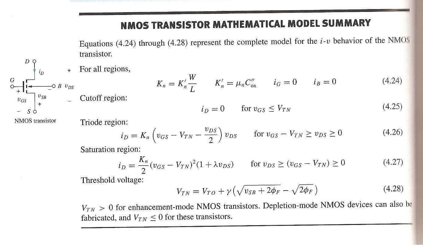
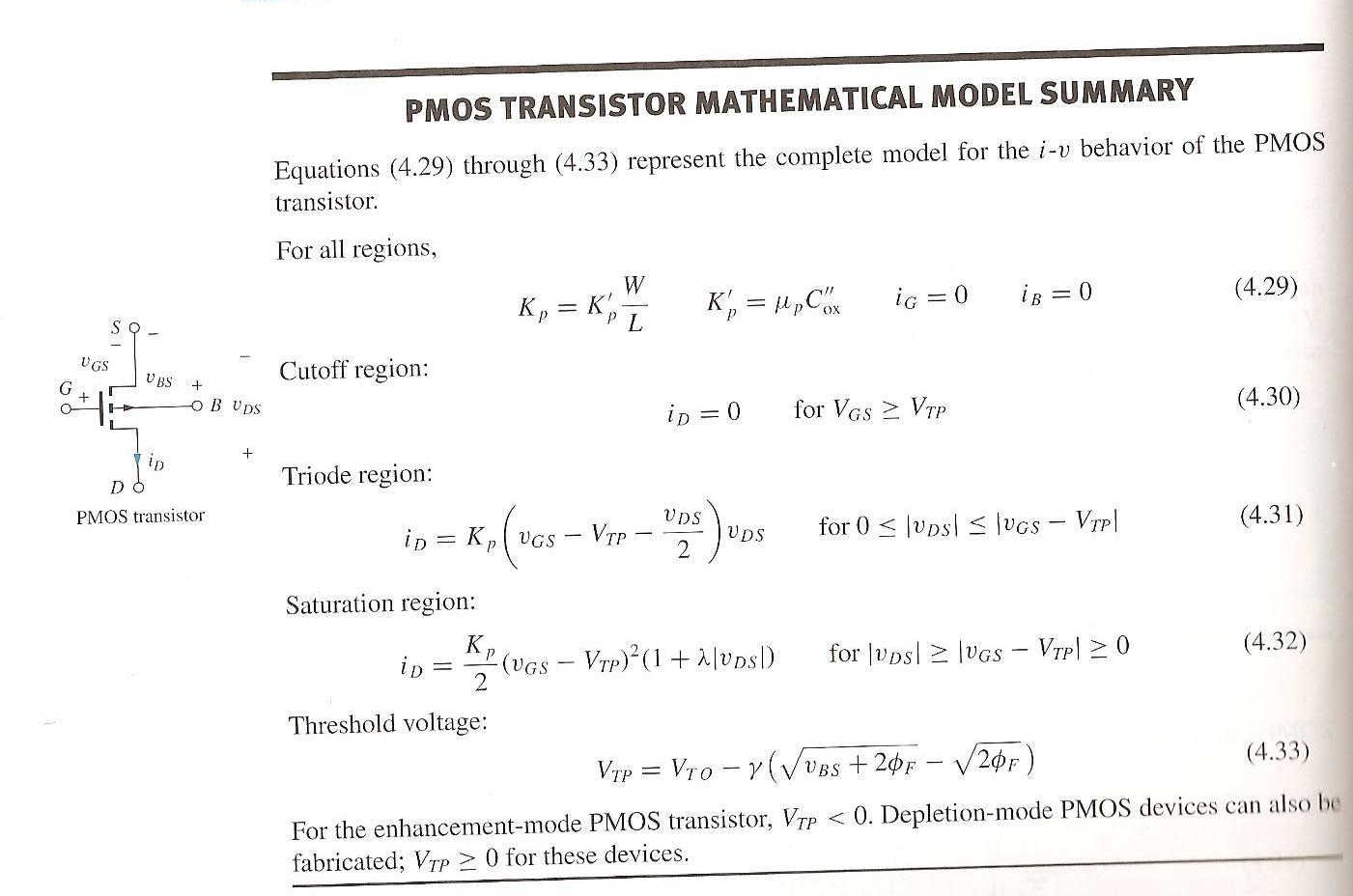
NOTE 1: Table 4.6 on Page 204
provides useful generic FET specifications information. If
these data are not provided in any of the Chapter 4 text problems, use
information in Table 4.6. Also the
inside of the front cover has all sorts of useful data. Just below Table 4.6 on Page 204, you will
also find some key constants.
Note 2: I also want to call your attention to the
following link from our WEB page FETNMOSSummary.jpeg and FETPMOSSummary.jpeg
Note 3: Be sure your WEB browser displays symbol
font correctly.
1.
Text Problem 4.1 (Just look at Figure 4.2) and Problem
4.2, and for 4.2 observe that this is
Cox, capacitance per unit area. A bit of modest plug-and-chug. Watch your units. Usually capacitance/cm2
are preferred for the capacitance per unit area units. When the text and in the
industry talks about an MOS capacitor, they are usually referring to capacitance/unit
area. The total capacitance can then be scaled by the W x L product. This idea of scaling is a very important VLSI
design concept. The parallel plate basic
capacitor model works well! We will also
soon observe how this plays into imaging and display applications.
2.
Text 4.4 and 4.8 for NMOS and Text 4.48 for
PMOS. Some additional basic calculations
to provide experience in units and nomenclature. Organize your results in a table. Page 160 (NMOS) and 162 (PMOS) has a table
defining the relationships for key FET model parameters. Refer to the WEB links in Note 2.
3.
Versions
of this problem have also been extracted from old quizzes. Refer to the sketch of an n-channel
enhancement-mode MOSFET fabricated in silicon. Assume room temperature
operation. Also assume
l = 0. Units are important.
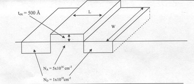
![]()
(a)
Compute
a value for Cox .
(b)
Compute
a value for the threshold voltage, Vt
using the threshold voltage graph posted on the WEB page.
(c)
Assume W/L = 10 and make reasonable
assumptions and/or use values from Table 4.6 for any other physical parameters
you may need. Compute values for “k”
and “KP” and then use your results from this part and Parts (a) and (b) to
generate a Shichmann-Hodges Level 1 model equation.
(d)
Using
your calculated results from Part (c), sketch and numerically label the iD versus vDS
as a function of VGS curves.
Label the Saturation, Cutoff, and Ohmic (Triode)
regions.
4. Text 4.18 NMOS . In addition to answering the problem questions,
refer to Text Figure P4.18 associated with Text Problem 4.18 and using the SPICE example I demonstrated in
class and the first part of Experiment 4, generate a SPICE NMOS model by
modifying the default NMOS transistor model (MBREAKN) that will reasonably match the curves
in P4.18 figure. If you look at the
curves, it is a good assumption that λ = 0. We will talk about λ on Friday, 26 February. Your problem submission must include the
listing of your modified MOS parameters and the resultant ID-VDS
curves as a function of VGS.
5. Text 4.49 PMOS In
addition to answering the questions, refer to Text Figure P4.49 associated with
Text Problem 4.49 and using the SPICE
example I demonstrated in class, generate a SPICE PMOS model by modifying the
default PMOS transistor that will match
the curves in P4.49 figure. We did not
generate the PMOS curves in Experiment 4, but the approach is similar. Observe that Figure P4.49 is given as a first
quadrant plot but the axes are labeled appropriately for the third
quadrant. Again, if you look at the
curves, it is a good assumption that λ = 0. We will talk about λ on Friday, 26
February. Your problem submission must
include the listing of your modified MOS parameters and the resultant ID-VDS
curves as a function of VGS. This will be a third-quadrant plot.
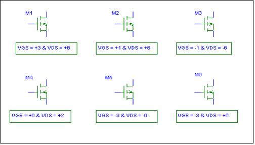
6. From an old quiz. Regions of operation are very important in
circuit design using MOSFETS. Extracted
from an old quiz. For the indicated bias conditions, state whether the FET
is operating in the OHMIC (TRIODE) region, SATURATION region, or CUTOFF region.
Explain your reasoning. Assume
that |VT | = 2
volts for both the NMOS and PMOS enhancement mode transistors.
M1
__________ M2 __________ M3 __________
M4 __________ M5
__________ M6 __________
This is what
we use for blocking dc and passing ac in many discrete device amplifier
circuits. Synonymous with coupling
capacitor. Also a dc blocking capacitor
is employed in your oscilloscope when switching to AC input using the soft
keys.
Consider the signal swing around the Q-Point which established the
dynamic range of a circuit
which we will use in amplifier design

Even though
you are an EE student, there is some information you can use from CS I. Of course, you can always dive deeper into CS
but it messy in more ways than one. I
don’t know if this diagram is covered in more advanced CS courses if you decide
to work on a CprE Minor. Can you tell that I am a hardware guy!