EE
2212
PROBLEM
SET 7
S.
G. Burns
Due: Wednesday, 23 March 2016
Problems 3 through 6 provide practice in working with
small-signal models. Use the basic voltage-controlled current generator FET
small-signal model with λ (Lambda) =0.
In addition to answering the text questions, you are to draw and label
the resultant small-signal model circuit diagram for Problems 3 through 6. Express your derivations symbolically; that
is no calculations are required. These four problems also will familiarize
you with the text FET symbol notation.
1. Refer
to Figure 6.17(d) on text page 306 and the more detailed version shown in
Figure 6.22(a) on page 315. Using the
data supplied in Figure 6.22(a), use a SPICE simulation to obtain a reasonable
match to the transfer characteristic shown in Figure 6.22(b). Submit your circuit diagram, FET model and
attribute data, and the transfer characteristic.
2. Extracted
and modified from an from an old quiz.
(a)
The
CMOS inverter consists of
(NMOS ENHANCEMENT MODE, NMOS DEPLETION 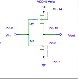 MODE, PMOS ENHANCEMENT MODE, PMOS DEPLETION MODE)
transistors. Circle your choices.
MODE, PMOS ENHANCEMENT MODE, PMOS DEPLETION MODE)
transistors. Circle your choices.
(b)
Sketch
and label the transfer characteristic.
Label the regions where M1 is ON and OFF, M2 is ON and OFF, the region where the circuit can
be used as an amplifier, the Q-Point yielding the highest power dissipation.
(c) The CMOS inverter static power dissipation
is (COMPUTED FROM THE SLOPE OF THE TRANSFER CHARACTERISTIC,ESSENTIALLY ZERO,
COMPUTED FROM P=(VI)/![]() ) . Circle your choice.
) . Circle your choice.
(d)
The
input resistance of a CMOS INVERTER is (ESSENTIALLY ZERO, COMPUTED FROM R=V/I,
Essentially ∞). Circle your
choice.
(e) You measured the output resistance of your CMOS
inverter in the 17 March lab. The
output resistance measured was (0 Ω, ∞ Ω, Tens of Ωs,
Several hundred Ωs, About 10 kΩ, About 2.2 MΩ)
The following two problems refer to switched capacitor design
discussed in our 4 March class.
3. Design a switched
capacitor circuit that could be used in place of a 10 kW resistor where the maximum frequency of any
signal does not exceed the typical audio
bandwidth of your smart phone Your
design should include:
· Well-labeled circuit diagram
· Key component values and an appropriate clock
frequency
· Waveforms as appropriate
4. Switched
Capacitor Low Pass Filter Design
Use the basic concepts from the 10 kΩ resistor design in Problem 3, you are to design a switched
capacitor LPF that replaces the analog LPF; a topology we studied extensively
the first couple of weeks of the semester.
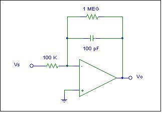
(a)
First recall the basics of
an analog LPF. Sketch and label the
voltage gain of this circuit, 20 log |A(jf)|. Refer to the first couple of weeks of the semester
when we studied active analog low-pass filters. Verify your results using a
SPICE simulation. Use a generic op amp
model. Include the SPICE-generated 20 log|Vo/Vs| vs. log(f) graph.
(b)
Redesign this circuit as a
switched capacitor low-pass filter. Your design should include:
· Well-labeled
circuit diagram.
· No
resistors-That is replace the two resistors with switched capacitors. Your
design should include appropriate W/L ratios.
You will end up requiring four FETs.
· An
appropriate clock frequency for operation at input signal frequencies to 10
kHz.
· Key
waveforms illustrating the operation.
The next problem requires use of the FET
small-signal model.
5. Text
13.5 and 13.8
as a combination. After you have
obtained the small-signal models, derive equations for the voltage gain defined
by av = vo/vi. Observe that no calculations
required. Note that this 13.5 uses an NMOS and
13.8 uses a PMOS.
Pot-Pourri From My Vast Files Of Stuff
For your
career and internship “guidance”
As
you can observe from my Google calendar I post on the WEB and on my door, I go to
lots of meetings, many with minimal You will also have many meeting
“opportunities” during your engineering
career. The following is so true: