EE 2212
EXPERIMENT 10
6 April 2017
BJT CURRENT SOURCES
LAST REMNDER
EXTRA CREDIT OPPORTUNITY: Up to 30 Points added to your end-of-the-semester Quiz Point
Total. How do you earn this? I want circuit diagrams
and specifications for power amplifiers and related equipment that you may have
for some of your “stuff” and is usable, that is, supports in-class
discussions when we get to power amplifiers towards the end of the
semester. Information such as circuit diagrams, specifications for
your sound systems, guitar amps, car stereos, powered sub-woofers,
associated power supplies, speaker systems, etc. I define power loosely
in that information on your portable electronics such as iPODs,mp3 players,
smart phones, tablets, etc. also is interesting to me and appropriate for class
discussion. I would like to borrow the material to supplement our class
discussions on power amplifier circuits. Do not just go to the WEB for
information that doesn’t relate directly to stuff you have. Hard Deadline
for receipt of materials is class on Monday, 10 April. Earlier is
better! Be sure your name is in the submitted materials. They will
be returned. I will award up to 30 points based upon relevance and
class usability and you describing the item and technical information to
the class. The meaner and badder the better.
Note 1: Report is due Thursday, 17 November.
Note 2: The CA 3046 is the same electrically as the
LM 3046. Just a different manufacturer.
Note 3: As usual, do not use the current mode on your
DMM because of issues with the internal fuse; measure the voltage drop across
the appropriate resistor and employ Ohm’s Law.
PURPOSE
The purpose of this experiment
is to build, model and characterize the
properties of a:
Ø Basic/Simple Current Source
Ø Widlar Current Source
COMPONENTS
Ø LM3046/CA3046 transistor array. The data sheet is posted on the class WEB
page
Ø Resistors and potentiometers as required
for the current sources.
PRELAB
Compute the values of the
resistors you will need to evaluate the simple and Widlar current sources at
the indicated current levels.
GENERAL INFORMATION
Ø In IC biasing networks, it is essential
that transistors be well matched and parameter variations track with
temperature. Figure 9.1 is a pin-out of
the LM3046/CA3046 Transistor Array. Observe that you MUST connect Pin 13, the
IC substrate, to the most negative point
in the circuit or bad things happen to the IC and the resultant fragrance in
the lab is unmistakable.
Ø The only reason there is a fixed 10 kW resistor in the circuit of Figure 9.2 is to protect the BJT against inadvertent
application of a high voltage across the
Base-Emitter junction as you adjust the potentiometer. You do not want to apply 15 volts to the base
of Q1 because the chip becomes toast (literally and figuratively)!!!
Again, bad things happen to the IC and
the resultant fragrance in the lab is unmistakable. Effectively, the series combination of the 10
kW resistor and the potentiometer is the RREF. Measure this total resistance value. You could substitute a fixed resistor of
approximately the same value for the potentiometer-R1 total.
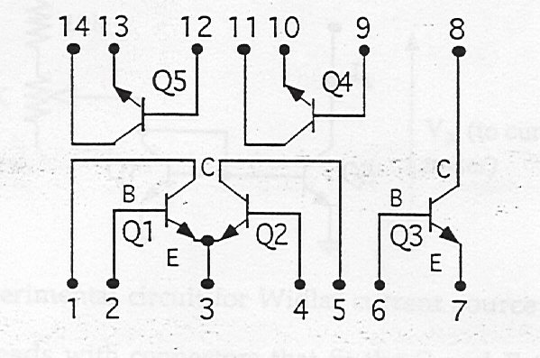
Figure 9.1 LM3046/CA3046 NPN
BJT ARRAY
SIMPLE CURRENT SOURCE
Figure 9.2 is a schematic
diagram of a simple current source.

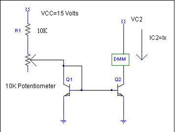
Connect the collector of Q2,
(VC2) to a 6-volt DC supply. Use
the DMM to measure the voltage drop, VR, across the 1 kΩ resistor and realize
that IC2 = VR/1 kΩ. Set IC2=IX to 1 mA by adjusting
the 10 kΩ potentiometer. Compare
this value to the reference current.
Measure all key currents and voltages. Construct the I-V output
characteristic by changing VC2 from 0 to 6 volts. Obtain the output resistance from the slope.
Compare to a SPICE simulation. Best
approach is to enter your data in an EXCEL spread sheet and let the graphing
function do all the “heavy lifting”. Of
course, use only data in the “flat” region.
WIDLAR CURRENT SOURCE
Figure 9.3 is a schematic
diagram of a Widlar current source.

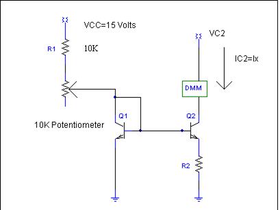
For a reference current of 1
mA, compute the value of R2 required to obtain Ix = 100 mA ±10%. Note that VCC = 15 volts. Now
connect the collector of Q2 (VC2) to a 6-volt DC supply. Use the
DMM to measure the voltage drop, VR, across the 10 kΩ resistor and realize
that IC2 = VR/10 kΩ.
You may have to change the value of R2 from the computed value to come within 100 mA ±10% .
Measure all key currents and voltages. Sketch the I-V output characteristic from VC2 from 0
to 6 volts.. Compare these results with the simple current source results. You will have to measure carefully because
the slope will be close to flat as you would expect. Again, best approach is to enter your data in
an EXCEL spread sheet and let the graphing function do all the “heavy
lifting”. Compare to a SPICE simulation.
Not quite a TESLA but getting
there

After All, This A Lab. How many of you have seen the cute cat
videos?

Enough Said!