EE 2212
EXPERIMENT 7
16
March
MOSFET Circuits
Report Due: Thursday,
23 March
Note:
EXTRA CREDIT
OPPORTUNITY: Up to 30
Points added to your end-of-the-semester Quiz Point Total. How do you
earn this? I want circuit diagrams and specifications for
power amplifiers and related equipment that you may have for some of your
“stuff” and is usable, that is, supports in-class discussions when we
get to power amplifiers towards the end of the semester. Information such
as circuit diagrams, specifications for your sound
systems, guitar amps, car stereos, powered sub-woofers, associated power
supplies, speaker systems, etc. I define power loosely in that
information on your portable electronics such as iPODs,mp3
players, smart phones, tablets, etc. also is interesting to me and
appropriate for class discussion. I would like to borrow the material to
supplement our class discussions on power amplifier circuits. Do not just
go to the WEB for information that doesn’t relate directly to stuff you
have. Hard Deadline for receipt of materials is class on Monday, 10
April. Earlier is better! Be sure your name is in the submitted
materials. They will be returned. I will award up to 30
points based upon relevance and class usability and you describing the item and
technical information to the class.
The meaner and badder the better.
PURPOSE
Ø NMOS Inverter with a Resistive Load
Ø NMOS Inverter with an Active Load
Ø CMOS Inverter
Ø CMOS Inverter Thevanin
Resistance Measurement
COMPONENTS
Ø CD4007 MOSFET array
Ø 0.01mF capacitor
Ø 3.3 kW and 100 W resistors
PRELAB
The device you will use
throughout this experiment is a CD4007B Transistor array. It contains three
N-channel and three P-channel devices connected as shown. Detailed schematic diagrams and pinouts are
available on the data sheet and also given below. Please use care when working with these
chips. They are very susceptible to excessive voltage and ESD (Electro-Static
Damage). Do not exceed the experiment
settings in an attempt to make your experiment work. The pin
configuration is given in Figure 7.1.
Note that you will be using the CD4007B which have a lower maximum
voltage rating than the CD4007UB. The
diagrams are the same for both the “B” and “UB” suffix devices. Avoid exposing the chip to ESD (electrostatic
damage). This time of the year often has
low relative humidities which make ESD more of an
issue. Do not exceed the VDD
maximums!!!
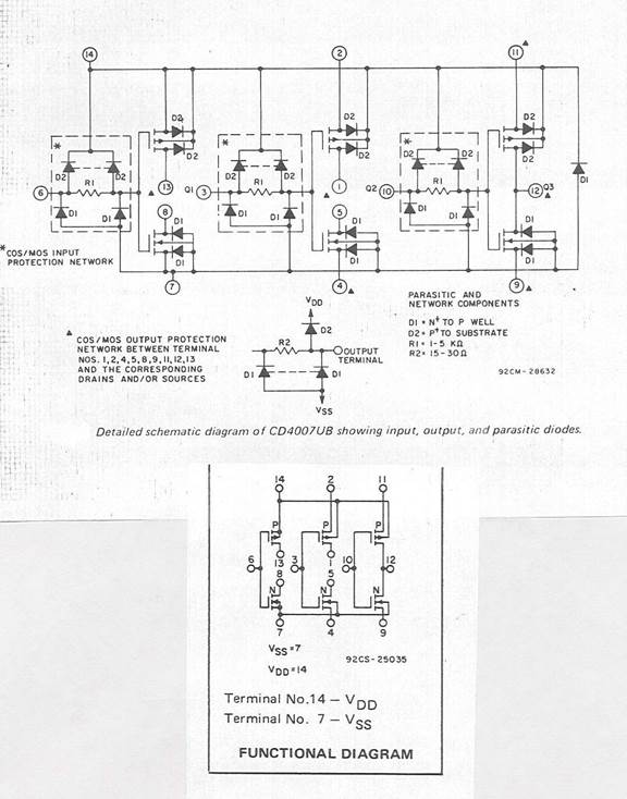
Figure 7.1 Pin Configuration of CD4007.
Warning: Pin 14 should always be connected to the
most positive dc voltage in the circuit.
Pin 7 will always be connected to the most negative dc voltage in the
circuit
(or
else ![MCBS00726_0000[1]](Experiment7MOSCircuits_files/image004.gif) )!!!
)!!!
PROCEDURE
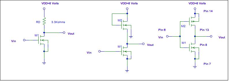
INVERTER CIRCUITS
Refer to the three circuit diagrams
in Figures 7.2, 7.3, and 7.4. All will operate with a VDD = +8 volt power
supply. Remember Pin 14 should always be
connected to the most positive dc voltage in the circuit. Pin 7 will always be connected to the most
negative dc voltage in the circuit.
You will need to arrange for an
offset voltage from the signal generator so that Vin
does not go below zero volts.
To standardize on the SPICE
simulations, use VTO = 2 volts for the NMOS and -2 volts for the PMOS; λ=
0.02 volts-1, and KP = 50E-3.
The default KP does not have enough gain to obtain the results I want.
Use default values for all other SPICE model parameters.
1. Set up the NMOS Inverter with a Resistive
Load as shown in Figure 7.2. Use the NMOS FET connected to CD4007 M1 Pins 6, 7,
and 8. Before connecting your function
generator to the circuit input, adjust it for a 0-8 V triangular waveform at a
frequency of 1 kHz. You will need to use the dc-offset control on your function
generator to do this. That is an 8 volt peak-to-peak triangular wave added to a
4 volt dc offset. Plot the transfer
characteristic, that is Vout versus Vin. Connect the input and output to the horizontal and
vertical inputs (respectively) of your oscilloscope set to the x-y mode. This
arrangement allows you to display the transfer characteristic of the
circuit. Identify the saturation, ohmic, and cutoff regions of operation. Suggest a Q-point
to obtain the largest small-signal voltage gain. Verify your experimental
results with a load line and SPICE simulation.
Observe that you will need to provide a dc offset from the signal
generator.
2. Set up the actively-loaded NMOS Inverter as
shown in Figure 7.3. Use CD4007 M1 Pins
6, 7, and 8 and M2 Pins 3, 4, and 5. Before
connecting your function generator to the circuit input, adjust it for a 0-8 V
triangular waveform at a frequency of 1 kHz. You will need to use the dc-offset
control on your function generator to do this. That is an 8 volt peak-to-peak
triangular wave added to a 4 volt dc offset.
Connect the input and output to the horizontal and vertical inputs
(respectively) of your oscilloscope set to the x-y mode. This arrangement
allows you to display the transfer characteristic of the circuit. Plot the transfer characteristic. Identify
the saturation, ohmic, and cutoff regions of
operation for each FET. Suggest a Q-point to obtain the largest small-signal
voltage gain. Verify your experimental results with a “load line” which
consists of the amplifier characteristic and SPICE simulation.
Compare your results with the resistively-loaded circuit. Observe that you will
need to provide a dc offset from the signal generator.
Note
that this circuit is different than the depletion mode inverter circuit discussed and SPICE simulation demonstrated in class.
![]()
Figure 7.2 NMOS Inverter Resistive Load Figure 7.3 NMOS Inverter Active Load Figure 7.4 CMOS Inverter
3.
Connect the CMOS inverter circuit of Figure 7.4.
with the CD4007 pins shown. You can also use the CMOS inverter FETS
connected using Pins 9, 10, 11, and 12.
Connect the input and output to the horizontal and vertical inputs
(respectively) of your oscilloscope set to the x-y mode. This arrangement
allows you to display the transfer characteristic of the circuit. Before
connecting your function generator to the circuit input, adjust it for a 0-8 V
triangular waveform at a frequency of 1 kHz. You will need to use the dc-offset
control on your function generator to do this. That is an 8 volt peak-to-peak
triangular wave added to a 4 volt dc offset.
Observe and sketch the transfer characteristic, recording all critical
values of voltage. Your report should
include a PSPICE simulation of this circuit using NMOS and PMOS models. Compare to the 4007 curves on the data sheets.
4.
Refer
to Figure 7.5. The same circuit as
Figure 7.4 but with a 0.01 μF capacitor
load. Measure the pulse response of the CMOS
inverter with a capacitor Co that has been added from the output to
ground to “slow down” the output waveform so that measurements can be more
easily made. Since the input of a CMOS gate is primarily capacitive, this also
will provide the output behavior when a CMOS gate is driving many other CMOS
gates (a capacitive load). Adjust your function generator to 0 to 8V square
wave at a frequency of about 10 kHz, then connect it to the input. Measure the
rise and fall times of Vout(t). You should be able to compute the effective value of
the CMOS inverter output resistance, Req,
from the rise and fall time measurements.
Refer to what you did in Experiment 1 for a basic RC network and design
equations. Compare your measured results
with a PSPICE simulation.
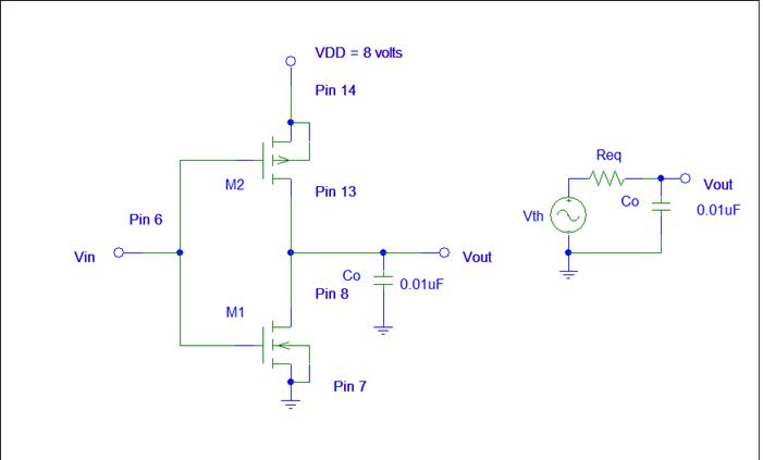
Figure 7.5 Circuit and Technique For Measuring Req (Thevanin Resistance)
A few more items to think about.
Compare the static power dissipation of the three circuits CMOS Inverter, NMOS Inverter
with a resistive load, NMOS inverter with an active load when operated as
switches/inverters as opposed to amplifier operation.
These Cartoons Represent EE at
its Finest!

![]()