EE
2212
PROBLEM
SET 7
S.
G. Burns
Due: Wednesday, 22 March 2017
Note: Problem Set 7 IS NOT due the Wednesday, 15
March, after break! Problem Set 7 and
the associated Quiz 7 due the following Wednesday, 22 March.
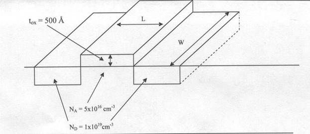
1. Versions of this problem have also been extracted from old quizzes. Refer to the sketch of an n-channel
enhancement-mode MOSFET fabricated in silicon. Assume room temperature
operation. Also assume
l = 0. Units are important.
(a) through (d) are a modest sample of what
could asked about the operation and
physics of the NMOS and PMOS
![]()
(a)
Compute
a value for Cox .
(b)
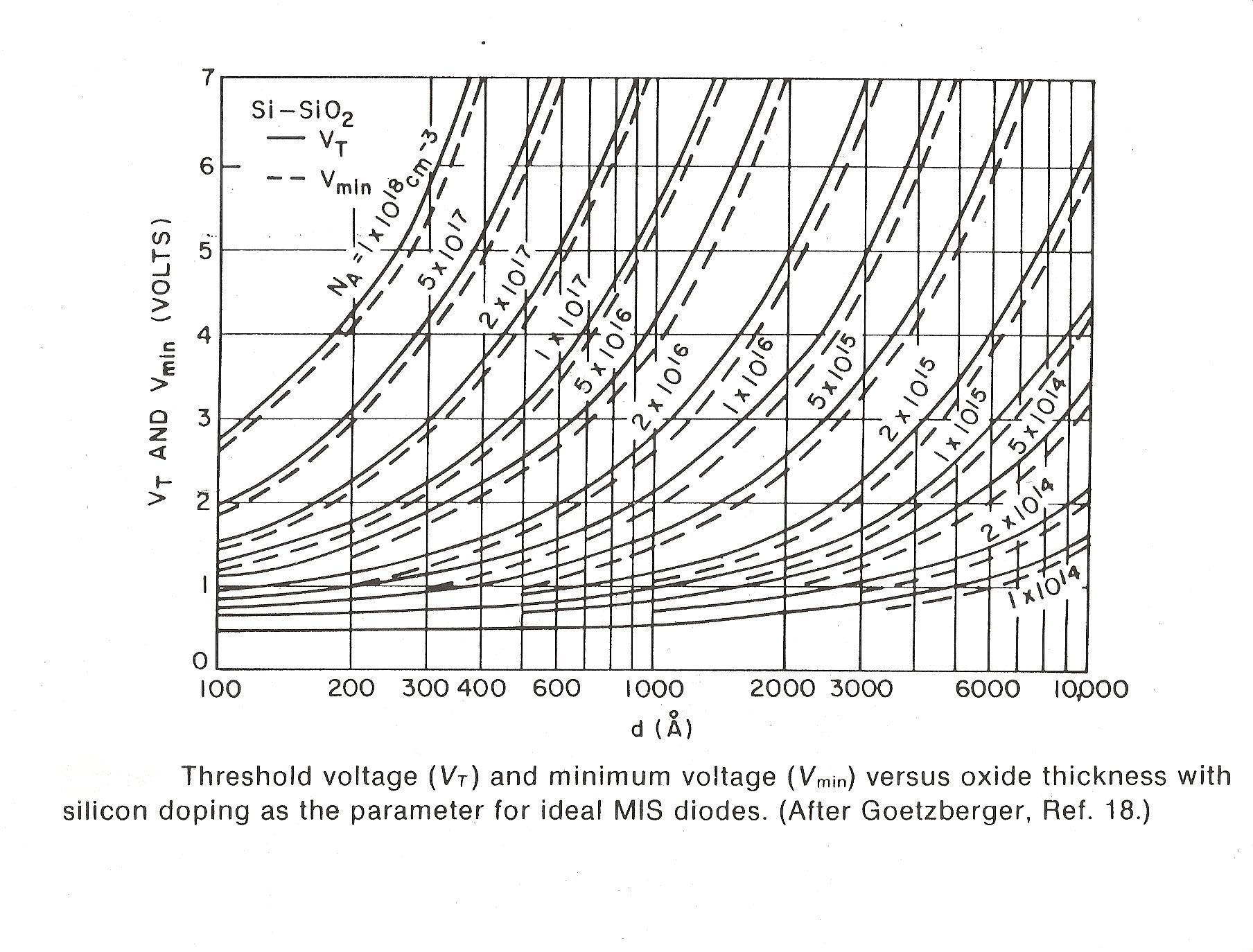
Compute
a value for the threshold voltage, Vt
using the threshold voltage graph posted on the WEB page ThresholdVoltageChart.JPG
(c)
Assume W/L = 10 and make reasonable
assumptions and/or use values from Table 4.6 on Page
203 for any other physical
parameters you may need. Compute values
for “k” and “KP” and then use your results from this part and Parts (a) and (b) to generate a Shichmann-Hodges Level 1 model equation.
(d)
Using
your calculated results from Part (c), sketch and numerically label the iD versus vDS
as a function of VGS curves. Label the Saturation, Cutoff, and
Ohmic (Triode) regions.
2. Similar
to the NMOS version from Problem Set 6. Text
4.48 PMOS. In
addition to answering the questions, refer to Text Figure P4.48 associated with
Text Problem 4.48 and using the SPICE
example I demonstrated in class, generate a SPICE PMOS model by modifying the
default PMOS transistor
that will match the curves in P4.48 figure. We did not generate the PMOS curves in
Experiment 7, but the approach is similar.
Observe that Figure P4.48 is given as a first quadrant plot but the axes
are labeled appropriately for the third quadrant. Again, if you look at the curves, it is a
good assumption that λ = 0. Your
problem submission must include the listing of your modified MOS parameters and
the resultant ID-VDS curves as a function of VGS.
This will be a third-quadrant plot.
3. Refer
to Figure 6.21 on text page 306. Using the
data supplied in Figure 6.21 (a). Perform a SPICE simulation to obtain a reasonable
match to the transfer characteristic shown in Figure 6.21(b). Submit your circuit diagram, FET model and
attribute data, and the transfer characteristic.
4. Extracted
and modified from an from an old quiz.
(a)
The
CMOS inverter consists of
(NMOS ENHANCEMENT MODE, NMOS DEPLETION 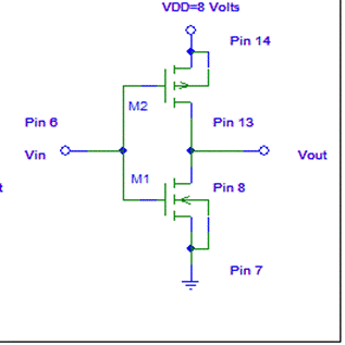 MODE, PMOS ENHANCEMENT MODE, PMOS DEPLETION MODE)
transistors. Circle your choices.
MODE, PMOS ENHANCEMENT MODE, PMOS DEPLETION MODE)
transistors. Circle your choices.
(b)
Sketch
and label the transfer characteristic.
Label the regions where M1 is ON and OFF, M2 is ON and OFF, the region where the circuit can
be used as an amplifier, the Q-Point yielding the highest power dissipation.
(c) The CMOS inverter static power dissipation
is (COMPUTED FROM THE SLOPE OF THE TRANSFER CHARACTERISTIC,ESSENTIALLY ZERO,
COMPUTED FROM P=(VI)/![]() ) . Circle your choice.
) . Circle your choice.
(d)
The
input resistance of a CMOS INVERTER is (ESSENTIALLY ZERO, COMPUTED FROM R=V/I,
Essentially ∞). Circle your
choice.
The following problem refer to switched capacitor
design which I anticipate discussing the week after break.
5. Switched Capacitor Low Pass Filter Design
Use the basic concepts from the resistor
design we will study the week after break, design a switched capacitor LPF that
replaces the analog LPF; a topology we studied extensively the first couple of
weeks of the semester.
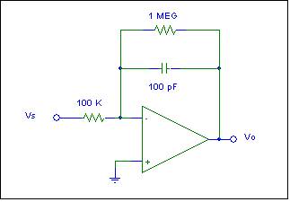
(a)
First recall the basics of
an analog LPF. Sketch and label the
voltage gain of this circuit, 20 log |A(jf)|. Refer to the first couple of weeks of the semester
when we studied active analog low-pass filters. Verify your results using a
SPICE simulation. Use a generic op amp
model. Include the SPICE-generated 20 log|Vo/Vs| vs. log(f) graph.
(b)
Redesign this circuit as a
switched capacitor low-pass filter. Your design should include:
· Well-labeled
circuit diagram.
· No
resistors-That is replace the two resistors with switched capacitors. Your
design should include appropriate W/L ratios.
You will end up requiring four FETs.
· An
appropriate clock frequency for operation at input signal frequencies to 10
kHz.
· Key
waveforms illustrating the operation.
Pot-Pourri From My Vast Files Of Stuff
For your
career and internship “guidance”
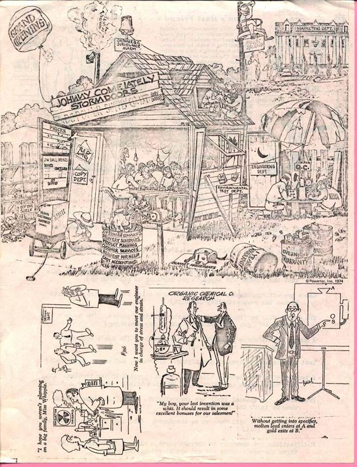
As you
can observe from my Google calendar I post on the WEB and on my door, I go to
lots of meetings, many with minimal utility.
You will also have many meeting
“opportunities” during your engineering
career. The following is so true: