EE 2212
PROBLEM SET 9
S. G. Burns
Due:
Wednesday, 5 April 2017
Note 1: REMNDER
EXTRA CREDIT OPPORTUNITY: Up to 30 Points added to your
end-of-the-semester Quiz Point Total. How do you earn this? I want
circuit diagrams and specifications for power amplifiers and
related equipment that you may have for some of your “stuff” and is usable, that
is, supports in-class discussions when we get to power amplifiers
towards the end of the semester. Information such as circuit diagrams,
specifications for your sound systems, guitar
amps, car stereos, powered sub-woofers, associated power supplies, speaker systems,
etc. I define power loosely in that information on your portable
electronics such as iPODs,mp3 players, smart
phones, tablets, etc. also is interesting to me and appropriate for class
discussion. I would like to borrow the material to supplement our class
discussions on power amplifier circuits. Do not just go to the WEB for
information that doesn’t relate directly to stuff you have. Hard Deadline
for receipt of materials is class on Monday, 10 April. Earlier is
better! Be sure your name is in the submitted materials. They will
be returned. I will award up to 30 points based upon relevance and
class usability and you describing the item and technical information to the class. The meaner and badder the better.
1. Draw and label the small-signal model for Figure P13.10
on page 830. Using your small-signal model, and by inspection,
estimate voltage gain. av = vO/vI. Observe the use of two dc supplies (independent
ideal voltage sources)!
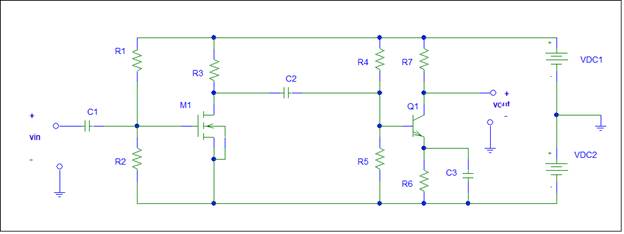
2. Draw and label the small-signal model for Figure P13.7 on
page 830. Using your small-signal model, derive an expression for the voltage
gain, av = vO/vI in terms of the circuit elements and model
elements. No numerical calculations! Observe that this is a pnp BJT which makes no difference when working with
the small-signal model.
3.
Small-Signal Analysis From An Old Quiz
Assume that for the BJT, VA is
finite and for the MOSFET, l is non-zero. Assume the capacitors are considered large at
the frequency of interest. Sketch and
label the small-signal model for this circuit. Observe, there are no
calculations required; only a carefully and thoroughly labeled small-signal
circuit.
4. We
are covering this topic Friday which may continue into Monday’s class. This will also be the foucus
of the 6 April Laboratory.
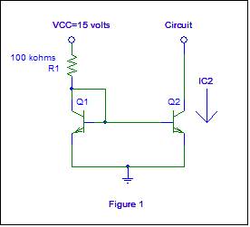
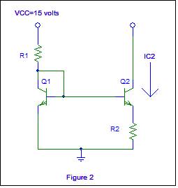
Simple and Widlar
Current Sink and Source Calculations
(a)
Compute a value for IC2 which is the
current you would sink from a circuit requiring that current bias level.
(b)
Design a pnp circuit
based upon the npn circuit shown in Figure 1 that
would operate as a current source, rather than a current sink, for the current
computed in Part (a). Your design must include a well-labeled circuit diagram.
(c)
Design a Widlar current
source to sink the current computed in Part (a). Refer to Figure 2. You have a
fair amount of flexibility
5. Text
16.8 Only Part (b) and assume λ
= 0. This is an NMOS current mirror system. “One liner” of arithmetic without a
calculator”!
6. NMOS
Current Mirror System. Similar to Problem 5 with some added wrinkles.
Once you realize that ID2 = 50 μA the problem can be done by inspection, or at most
on one line, without a calculator! Several elements of this problem were used
on an old quiz.
![]()
![]()
![]()
![]()
![]()
![]()
![]()
![]()
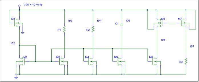
Assume the following:
(a) M1 and M2 are matched
(b) l = 0 for all MOSFETS (c) L identical for all FETS. (d) ID2 = 50 μA.
(e) W1=W2=W3=W6=W8 (f)
W4=W5=2 x W2 (g) W7 = 3 x W8 (h) Except for W/L ratios, the fabrication process
are the same for all FETs.
Pay attention to sign
conventions!
Provide values for:
ID3 =__________________
ID4 = ____________________ ID7 ________________
ID5 = _________________
(Trick question. Careful-look at the drain circuit for M5!