EE 2212
EXPERIMENT 11
12 April 2018
THE EMITTER-COUPLED PAIR
Report Due: 18 April 2018
Note: Since we are close to
the end of the semester, late reports will not be accepted.
PURPOSE
Ø The purpose of this experiment is to characterize
the properties of an emitter-coupled
pair:
·
DC
Transfer Characteristics
·
Time
Domain Measurements
(COMPONENTS
Ø
LM3046/CA3046
transistor array. The data sheet is
posted on the class WEB page LM3046NationalSemiconductor.pdf
Ø
20
kW resistors for the collector resistors which should be
reasonably well matched. Check with the
DMM.
Ø
4.7
kW resistor for the input voltage divider
Ø
47 W resistor for the input voltage divider
GENERAL INFORMATION
Ø In IC biasing networks, it is essential
that transistors be well matched and parameter variations track with
temperature. Figure 11.1 is a pin out
of the LM3046/CA3046 Transistor Array. Observe that you MUST connect Pin 13,
the IC substrate, to
the most negative point in the circuit or bad things happen to the IC. The most negative point is the VEE-REE
node, not ground!.
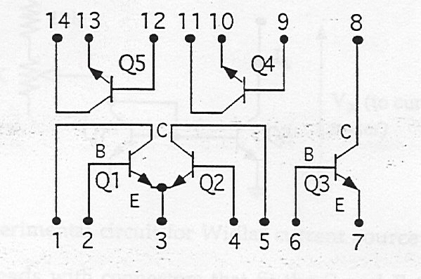
Figure 11.1 LM3046/CA3046 NPN
BJT ARRAY
Use Figure 11.2 and class notes for guidance to
prepare a detailed circuit diagram.
Include pinouts for the LM3046/CA3046 npn
array. From your circuit diagram and circuit specifications, calculate the expected
important Q-point values and Adm
.
DC MEASUREMENTS
Refer to the diagram and data
sheet of the LM 3046/CA3046 BJT array.
Set up the circuit in Figure 2 using Q1 and Q2 for
the emitter-coupled pair. Select a value
for REE such that the DC values for Vo1 and Vo2 are about 5 volts. Ground both the inputs of Q1 and Q2.
Measure the all Q-point voltages and currents using the DMM. Use the oscilloscope to also check for excessive
noise which may translate as a noisy dc voltage measurement. Pay particular attention to VOD.
Since the transistors and resistors are reasonably well matched, you would
expect VOD = 0 or reasonably close. If VOD is larger than
a few tens of mV, check your circuit and/or match the collector resistors
better. Lead dress and length is also
important. Be neat! Compare your Q-point values with the expected
and PSPICE simulations. In addition to
using the DMM, look for excessive noise using the scope even though you are
measuring a dc voltage.
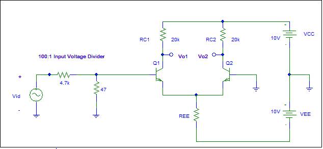
Figure 11.2
TRANSFER CHARACTERISTICS
The transfer characteristics of
a circuit can be displayed using the X-Y oscilloscope inputs. The amplitude of
the input must be large enough to drive the input through the entire desired
range of operation. You are particularly interested in the VOD
versus VID characteristic. Use a low frequency sinusoid or
triangular wave as the input. From a practical viewpoint, if the input signals
are noisy because of low amplitudes, you will choose to use an input voltage
divider to provide "cleaner" waveforms. Note the 100:1 voltage divider input drive
circuit shown in Figure 2, although it
doesn’t have to be 100:1. The signal
generators have a 100 mV minimum. By
using a 100:1 external divider, you can achieve a relatively noise free signal
at the input to the BJT bases. Keep
track of the divider ratio you finally use to scale your measurement correctly.
Also observe that because the oscilloscope does not have a floating input
(i.e., one side of each of the two oscilloscope inputs are connected to ground), you will have to
measure either VO1 or VO2 and scale the final results
accordingly by a factor of 2 and also do not forget the sign (180°phase)
differences for each of the outputs.
Show that the slope of the
transfer characteristic will be equal to |Adm/2|.
Compare your results to a SPICE simulation.
DIFFERENTIAL-MODE OPERATION
Set up your input signals, use
1 kHz, so that the output is reasonably linear. You will need some level of
voltage division as shown in Figure 2.
Figure 2
illustrates a 100:1 divider but the actual divider value is not
critical. Use the oscilloscope and DMM
to measure the differential-mode voltage gain. Compare your results to your
calculations and a SPICE simulation.
A bit of EE humor.

This guy deserves a tip!
And for those of you who go to
Buffalo Wild Wings and
try their “Blazin”
ghost pepper suace

You might cover conformal
mapping from an advanced math course
when using Smith
Impedance Charts
in EE 3445 or the Antenna and Transmission
Line Course
