EE 2212
EXPERIMENT 9
8 April 2021
BJT CURRENT SOURCES
Report Due:
15 April
Note 1: The
CA 3046 is the same electrically as the LM 3046. Also the 3045 is also the same electrically Just a different manufacturer.
Note 2: As usual,
do not use the current measurement mode on your DMM because of issues with the
internal fuse; measure the voltage drop across the appropriate resistor and
employ Ohm’s Law.
Note 3:
This is the last experiment that will be collected and graded this
semester.
PURPOSE
The purpose of this experiment is to build, model
and characterize the
properties of a:
Ø Basic/Simple
Current Source/Sink
Ø Widlar Current Source/Sink
COMPONENTS
Ø LM3046/CA3046/3045 transistor
array. LM3046NationalSemiconductor.pdf The data sheet is also posted on the class WEB
page
Ø Resistors
and potentiometers as required for the current sources.
PRELAB
Compute the values of the resistors you will need
to evaluate the basic/simple and Widlar current
sources at the indicated current levels.
GENERAL
INFORMATION
Ø In
IC biasing networks, it is essential that transistors be well matched and
parameter variations track with temperature.
Figure 9.1 is a pin-out of the LM3046/CA3046 Transistor Array. Observe
that you MUST connect Pin 13, the IC substrate, to the most negative point in
the circuit or bad things happen to the IC and the resultant fragrance is
unmistakable.
Ø The
only reason there is a fixed 4.7 kW resistor
in the circuit of Figure 9.2
is to protect the BJT against inadvertent application of a high voltage across the Base-Emitter
junction as you adjust the potentiometer.
You do not want to apply 9 volts to the base of
Q1 because the chip becomes toast (literally and figuratively)!!! Again, bad things happen
to the IC and the resultant fragrance is
unmistakable. Effectively, the series
combination of the 4.7 kW resistor
and the potentiometer is the RREF.
Measure your total resistance value.
You could substitute a fixed resistor of approximately the same value
for the potentiometer-R1 total if that is more convenient.
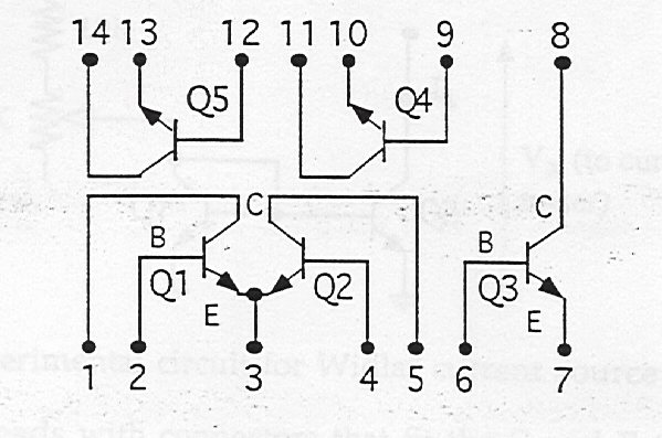
Figure 9.1 LM3046/CA3046 NPN BJT ARRAY
SIMPLE
CURRENT SOURCE/SINK
Figure 9.2 is a schematic diagram of a simple/basic current
source/sink.

Figure 9.2 Simple/Basic Current Source
·
You will be using the DMM function on the HANTEK
for this experiment
·
The simple/basic current source/sink will use Q1
and Q2 on the 3046/3045
·
Set R1 and R2 such that IC1 is about 1 mA. This is your reference current and will
mirror to Q2 which is what you will
experimentally verify
·
Adjust VCC2 over the entire range of 0 to 9
volts. Measure VCE2 at Pin 5 and IC2 by
measuring the voltage drop across R3 and applying Ohm’s Law. Measure as many data points as you deem
necessary to get the “constant current source” characteristic.
·
Use EXCEL to record your data and plot IC2 as a
function of VCE2
·
Obtain the output resistance from the slope.
Compare to a SPICE simulation using the generic npn model which allows you to modify VAF and BF to
fit your results. Best approach is to
enter your data in an EXCEL spread sheet and let the EXCEL graphing function do
all the “heavy lifting” of a linear regression. Of course, use only data in the “flat” region
to obtain the output resistance.
WIDLAR
CURRENT SOURCE
https://en.wikipedia.org/wiki/Bob_Widlar
Figure 9.3 is a schematic diagram of a Widlar current source.
We will use Q3 and Q4 on the 3046/3045 since the
emitters of Q1 and Q2 are connected together internally.

Figure 9.3 Widlar
Current Source
·
You will be using the DMM function on the HANTEK
for this experiment
·
The Widlar current source/sink will use Q3 and Q4 on the
3046/3045
·
Set R5 and R6 such that IC1 is about 1 mA. The same settings you used for Figure 9.2
should still work.
·
For a reference current of 1 mA, compute the value
of RW required to obtain IC4 = 100 mA ±10%. Note that VCC = 9 volts.
·
Adjust VCC2 over the entire range of 0 to 9
volts. Measure VC2 at Pin 11 and IC2 by
measuring the voltage drop across R8 and applying Ohm’s Law. Measure as many data points as you deem
necessary to get the “constant current source” characteristic.
·
Use EXCEL to record your data and plot IC2 as a
function of the voltage at Pin 11
·
Obtain the output resistance from the slope.
Compare to a SPICE simulation using the generic npn model which allows you to modify VAF and BF to
fit your results. Best approach is to
enter your data in an EXCEL spread sheet and let the EXCEL graphing function do
all the “heavy lifting” of a linear regression.
Of course, use only data in the “flat” region to obtain the output
resistance.
As an engineering student, you may be asked and
expected to fix your parent’s television and other techno toys over
Summer break or you don’t get to
eat any home cooking and you will sleep on the garage floor.

A UROP suggestion.

Start thinking about Senior Capstone Design!

