EE
2212
PROBLEM
SET 3
S.
G. Burns
Due: Monday, 15 February
Note 1: I strongly encourage you
to study the Semiconductor supplement I posted SemiconductorDeviceProcessingSupplementTextSection2.11.pptx in preparing for Quiz 3 and to assist you
with this problem set.
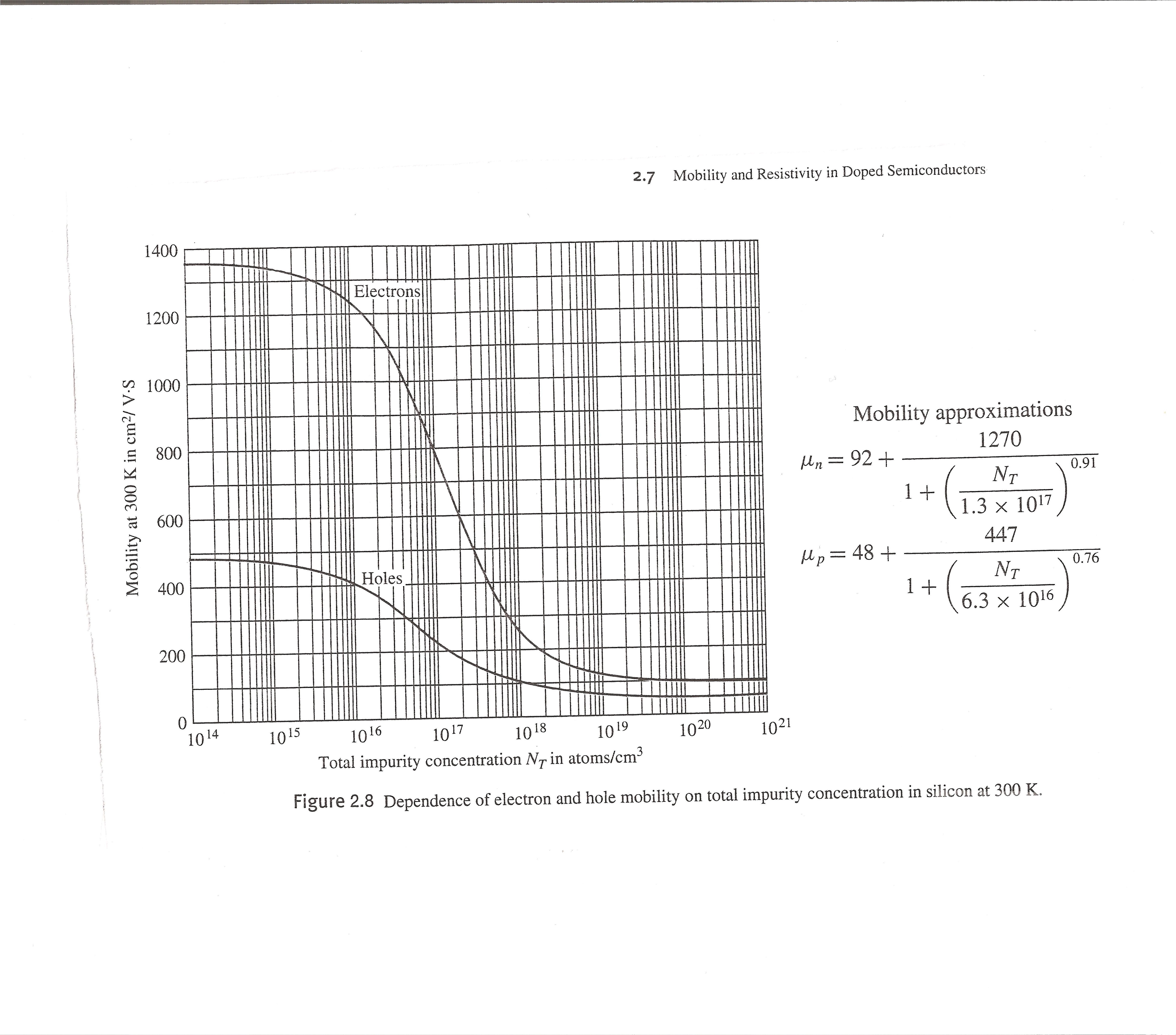
Note 2: Use Figure 2.8 on Text Page 55 for obtaining
mobilities. Do not use the empirical “curve-fit” formulas next to Figure 2.8. By using
graphs and curves, you do not have to perform any algebraic messy calculations
using the polynomial curve fits.!!!
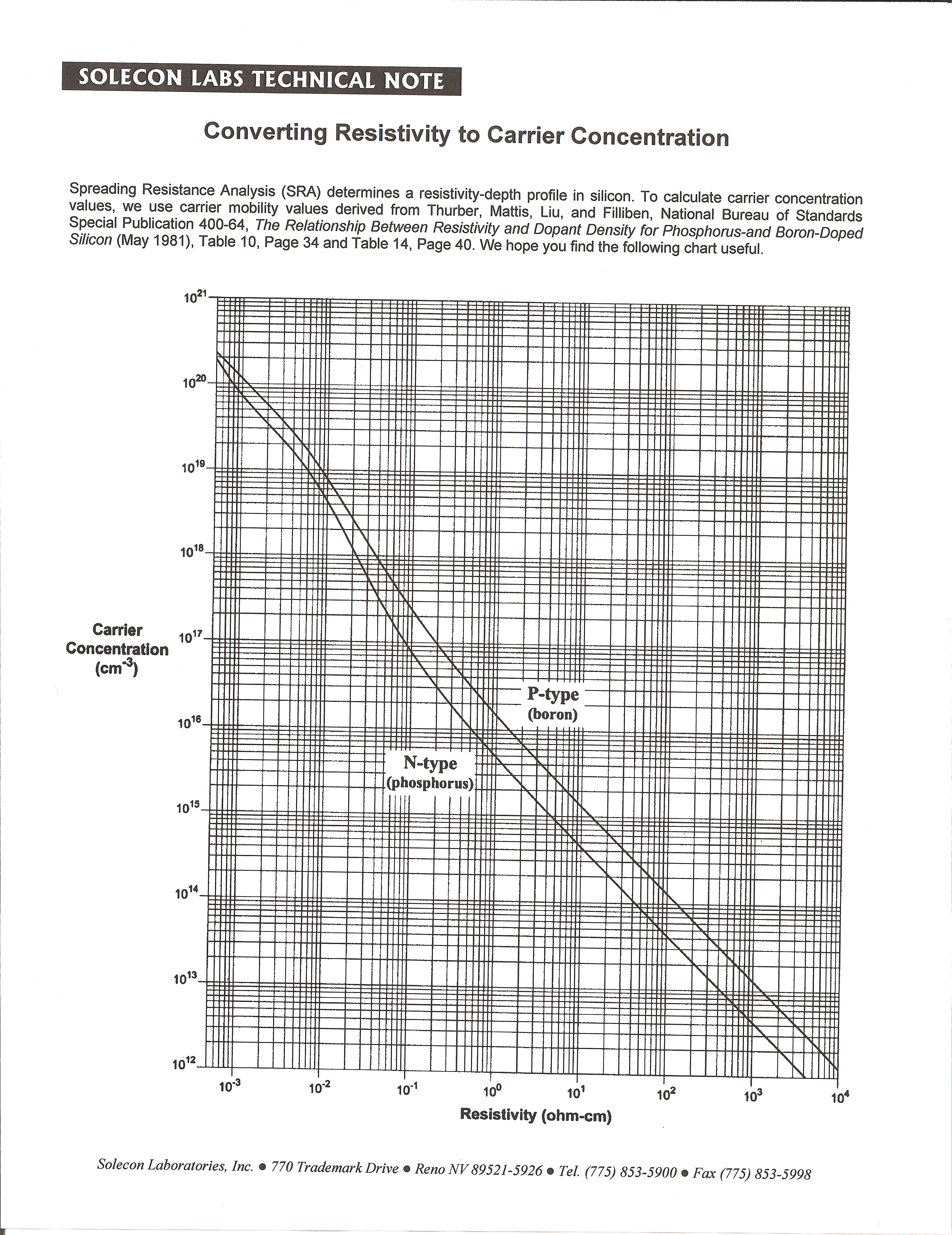
Note 3: Use the Solecon
curves Solecon.JPG
posted on the EE 2212 WEB page for resistivities,
ρ.
Observe that the Solecon curves use log-log scales and Figure 2.8 Mobility.JPG use semi-log scales. If you are unfamiliar on
how to read the log-log or semi-log scales on these types of graphs, ask.
Note 4: General material conductivity given by ConductivityRev1.jpeg
1. Text Problems 2.30 and 2.31
2. From
an amalgamation of old quiz problems and using concepts in Text Problems 2.30 and 2.31. You are to evaluate the properties of a
resistor fabricated from a rectangular
solid piece of doped Si.
W = 0.5 mm,
T = 100Å, and L = 10 mm.
Use the Solecon resistivity curves and the
text mobility curves. Assume ni=
1.0 x 1010 cm-3 (refer to the table on the inside front cover
although many references and graphs show this as ni=
1.5 x 1010 cm-3) Units are important!
(a) Fill in the Table Assume the rectangular solid is donor doped
Si doped with ND = 3 x 1017cm-3
|
PROPERTY |
ANSWER |
|
List two possible donor dopants |
|
|
Majority Carrier Type and Density |
|
|
Minority Carrier Type and Density |
|
|
Resistivity |
|
|
Mobility |
|
|
Resistance between Terminals A and B |
|
(a)
Fill in the Table Assume the
rectangular solid is now acceptor doped Si doped with NA= 3 x 1017cm-3
|
PROPERTY |
ANSWER |
|
List two possible acceptor dopants |
|
|
Majority Carrier Type and Density |
|
|
Minority Carrier Type and Density |
|
|
Resistivity |
|
|
Mobility |
|
|
Resistance between Terminals A and B |
3. Resistor
Design and Analysis
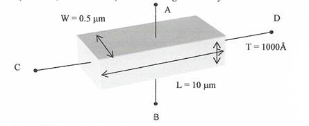
(a)
Estimate the mobility, μ, and the
resistivity, ρ, if this resistor were fabricated from phosphorus-doped Si where ND
= 3 x 1017 cm-3.
Also compute the value of the
resistance obtained
between terminals C and D
and A and B.. Use graphs.
(b)
Estimate the mobility, μ, and the
resistivity, ρ, if this resistor were fabricated from boron-doped Si where
NA = 3 x 1017 cm-3. Also compute
the value of the resistance obtained between terminals C and D and A and B.. Use graphs.
4. Refer
to Table 2.3, page 44 in the text. Watch
your units!
(a)
Compute the wavelength for a photon emitted
from GaAs, GaN, and InP
and indicate their relationship to the wavelengths associated
with the human visual optical
spectrum.
(b) Suppose you had the
design responsibility to bandgap engineer a semiconductor material to provide
LASER optical emission for the applications listed below. Provide numerical values in eV for a material
band gap energy to meet these applications.
i.
DVD
players or a high end game console using
blue LASERS (i.e. SONY BLU-RAYTM DVDs or HD Format DVDs)
ii.
A CD player solid-state LASER operating in the near-infrared. Of course CDs are rapidly becoming obsolete.
iii.
Green LASER pointer.
iv.
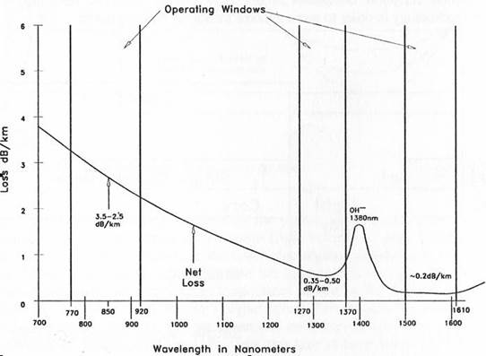
Lowest loss
optical fiber spectral window for
contemporary optical fiber transmission lines.
Use the graph below.
NOW
FOR THE IMPORTANT STUFF
For those
of you contemplating doing some house wiring:
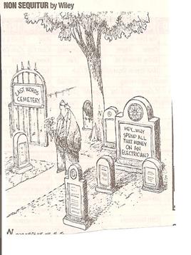
Chapter 2 Support.
In recognition of our study of semiconductor physics or
what physics majors call “condensed
matter physics”.


And we don’t want to forget concepts learned in
Physics 1

Just so
you don’t forget Ohm’s law
And this follows nicely with our Chapter 2
discussions.
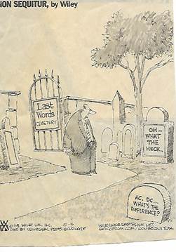
More Chapter 2 Support With
A Bit Of Trig To Help You Out