EE
2212
PROBLEM
SET 3
S.
G. Burns
Due: Wednesday, 8 February 2017
Note 1: I strongly encourage you
to study the Semiconductor supplement I posted SemiconductorDeviceProcessingSupplementTextSection2.11.pptx in preparing for Quiz 3 and to assist you
with this problem set.
Note 2: Use Figure 2.8 on Text Page 55 for obtaining
mobilities. Do not use the empirical “curve-fit” formulas next to Figure 2.8. By using
graphs and curves, you do not have to perform any algebraic messy
calculations!!!
Note 3: Use the Solecon
curves posted on the EE 2212 WEB page for resistivities,
ρ.
Observe that the Solecon curves use log-log scales and Figure 2.8 use semi-log
scales. If you are unfamiliar on how to
use the log-log or semi-log scales on these types of graphs, ask.
Note 4: FYI, Conductivity, σ, of Gold, Au, is
4.1 x 10⁵ [1/(Ω-cm)]
1. Integrated
circuit interconnect metallizations are often fabricated from Al, Cu, and Au. Gold (Au) has a conductivity σ = 4.1 x 10⁵ (W-cm)-1. Observe that this is a
bit higher than aluminum (Al). Use the Conductivity chart on the EE 2212 WEB
page. Fill in the table for a metal strip 0.25 mm wide, 3 mm long, and 300 Å thick? Provide one technical advantage and one technical disadvantage for
each material. Properties to consider
are melting point, cost, reactivity and corrosion resistance, processing
technology, etc. There are a number of
advantages and disadvantages; I am only asking for one in each case.
|
Material |
Resistivity, r |
Resistance, R |
Technical Advantage |
Technical Disadvantage |
|
Al |
||||
|
Au |
||||
|
Cu |
2. The
active conducting material in one of the resistors in the lab has a dimensions
L = 0.75 cm and
a radius of r = 1 mm and is fabricated from a material that has a conductivity of σ = 0.3 (Ω-cm)-1. Answer the following questions:
(a) Compute the value of the resistance.
(b) 5 volts are applied across the
resistor. What is the current density,
J, in the resistor?
(c) The lab resistors are rated at ¼
watt. For your calculations in Parts (a)
and (b), is the resistor operating within its power rating? Show your calculations.
(d) Your best friend electrical engineering
student from a large university in the Twin Cities, who is not doing very
well in their EE 2212 equivalent course, claims to have designed a
really low value resistor by changing σ where R= 10-5
Ω with these same dimensions.
Politely
explain why this is not possible.
3. Text
2.26 and 2.27
4. Resistor
Design and Analysis

(a)
Assume the resistor is fabricated from
gold, Au; an unlikely design approach,
compute the value of the
resistance obtained
between terminals C and D
and A and B.
(b)
Estimate the mobility, μ, and the
resistivity, ρ, if this resistor were fabricated from phosphorus-doped Si where ND
= 2 x 1017 cm-3.
Use graphs.
(c)
Estimate the mobility, μ, and the
resistivity, ρ, if this resistor were fabricated from boron-doped Si where
NA = 2 x 1017 cm-3. Use graphs.
5. Refer to Table 2.3, page 45
in the text.
(a)
Compute the wavelength for a photon emitted
from GaAs, GaN, and InP and
indicate
their relationship to the wavelengths associated with the optical spectrum.
(b) Suppose you had the
design responsibility to bandgap engineer a semiconductor material to provide
optical emission for the applications listed below. Provide numerical values in eV for a material
band gap energy to meet these applications.
i.
DVD players
using blue LASERS (i.e. SONY BLU-RAYTM DVDs or HD Format
DVDs)
ii.
A CD player solid-state LASER operating in
the near-infrared
iii.
Green LASER pointer.
iv.
Lowest loss
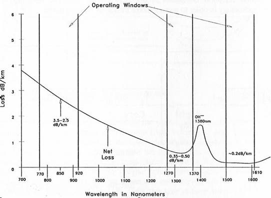
optical fiber spectral window for
contemporary optical fiber transmission lines.
Use the graph.
For those of you contemplating
doing some house wiring over spring recess.
Now for the really important stuff. In recognition of our study of some semiconductor physics
or what physics majors call condensed matter physics.


And we don’t want to forget concepts learned in
Physics 1
Just so
you don’t forget Ohm’s law
And this follows nicely with our Chapter 2
discussions.
More Chapter 2 Support With
A Bit Of Math To Help You Out